Organic luminous device

A technology of organic light-emitting device and organic light-emitting layer, which is used in the manufacture of electrical components, electrical solid-state devices, semiconductor/solid-state devices, etc.

Inactive Publication Date: 2014-01-22
华映视讯(吴江)有限公司 +1
View PDF6 Cites 4 Cited by
  • Summary
  • Abstract
  • Description
  • Claims
  • Application Information

AI Technical Summary

Problems solved by technology

However, this optical film can only avoid the reflection phenomenon between the substrate

Method used


Image

  • Organic luminous device
  • Organic luminous device

Examples


Embodiment Construction

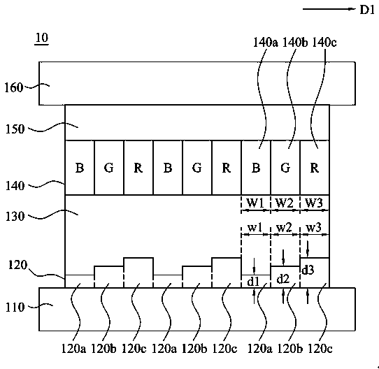
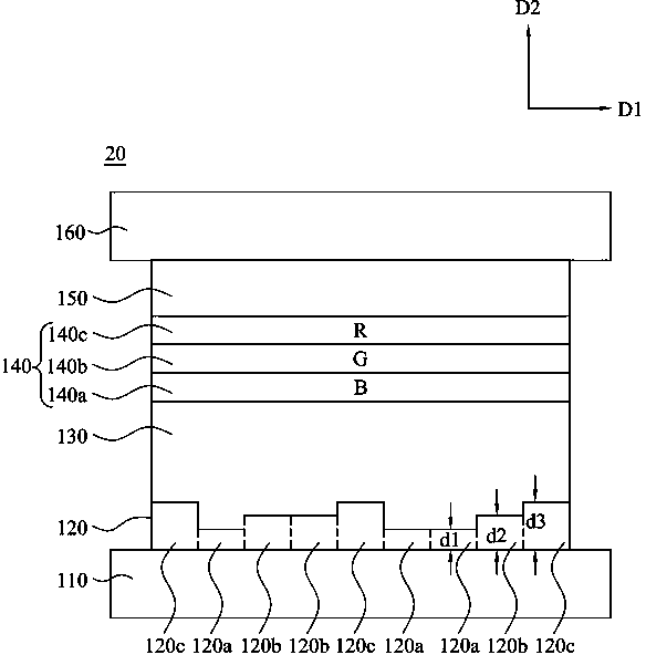
[0041] see figure 1 , figure 1 is a schematic cross-sectional view illustrating an organic light emitting device 10 according to an embodiment of the present invention. The organic light emitting device 10 includes a transparent substrate 110 , an intermediate layer 120 , a first electrode 130 , an organic light emitting layer 140 and a second electrode 150 .

[0042] The material of the transparent substrate 110 can be glass or plastic. Glass has a refractive index of about 1.52. The plastic can be, for example, acrylic resin (Acrylic), epoxy resin (Epoxy), polyethylene terephthalate (Polyethylene terephthalate, PET) or polycarbonate (Polycarbonate, PC), and its refractive index is about 1.49 to Between 1.6.

[0043] The first electrode 130 is located above the transparent substrate 110 . The material of the first electrode 130 can be, for example, indium tin oxide (Indium thin oxide, ITO) or other suitable transparent conductive materials. The refractive index of indiu...


PUM

PropertyMeasurementUnit
Thicknessaaaaaaaaaa

Abstract

The invention relates to an organic luminous device, which comprises a transparent base plate, a first electrode, an organic luminous layer, a middle layer and a second electrode, wherein the first electrode is positioned above the transparent base plate, the organic luminous layer is positioned above the first electrode and is used for sending out light in the first wave length, the second wave length and the third wave length, and the first wave length, the second wave length and the third wave length are mutually different. The middle layer is arranged between the transparent base plate and the first electrode in a clamping way, and the refractive index of the middle layer is in a range between the refractive index of the transparent base plate and the refractive index of the first electrode. The middle layer is provided with a first region, a second region and a third region ranged in a plane direction, the thicknesses d of the first region, the second region and the third region are respectively calculated according to the following formula that d=(2x+1) lambda/4n, wherein x is 0 or an integer, lambda is respectively the first wave length, the second wave length and the third wave length, and n is the refractive index of the middle layer. The second electrode is positioned above the organic luminous layer.

Description

technical field [0001] The present invention relates to a light-emitting device; in particular, an organic light-emitting device. Background technique [0002] Generally, an organic light emitting device includes a substrate, an anode, a light emitting layer and a cathode. The organic light-emitting device has the advantages of uniform light emission and low driving voltage, but its effective light utilization rate is low. This is because the light emitted by the light-emitting layer is easily reflected between the anode and the substrate or between the substrate and the air, resulting in part of the light being confined inside the anode or the substrate and unable to emit light, resulting in low effective light utilization. [0003] In order to solve the above problems, a layer of microstructured optical film can be pasted on the outside of the substrate to change the outgoing angle of light. However, this optical film can only avoid the reflection phenomenon between the...

Claims


Application Information

Patent Timeline
IPC IPC(8): H01L51/52H01L51/50
CPCH10K50/13H10K50/11H10K2101/10H10K50/858
Inventor 邱逸文刘胜发邱继毅黄檠裕
Owner 华映视讯(吴江)有限公司
Why Eureka
Try Eureka