Laminate and method for separating the same

Inactive Publication Date: 2012-05-17
TOKYO OHKA KOGYO CO LTD
View PDF6 Cites 37 Cited by
  • Summary
  • Abstract
  • Description
  • Claims
  • Application Information

AI Technical Summary

Benefits of technology

[0012]With the arrangement, the present invention can provide a laminate in which a target is

Problems solved by technology

However, a semiconductor wafer (hereinafter wafer) serving as a base of a chip gets thinner by polishing and decreases its strength, and consequently is more likely to be cracked or bended.
Fur

Method used


Image

  • Laminate and method for separating the same
  • Laminate and method for separating the same
  • Laminate and method for separating the same

Examples


examples

(Preparation of Laminate)

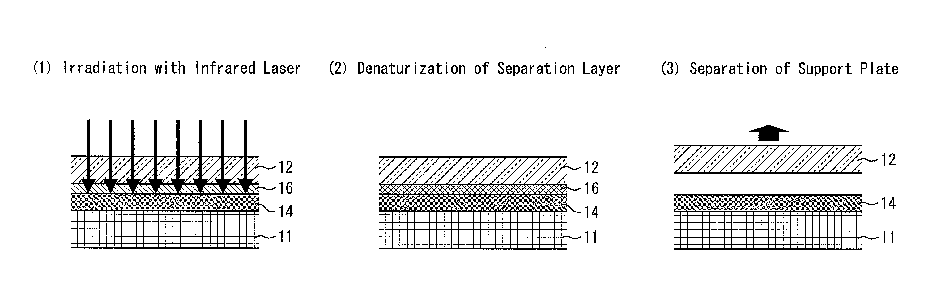
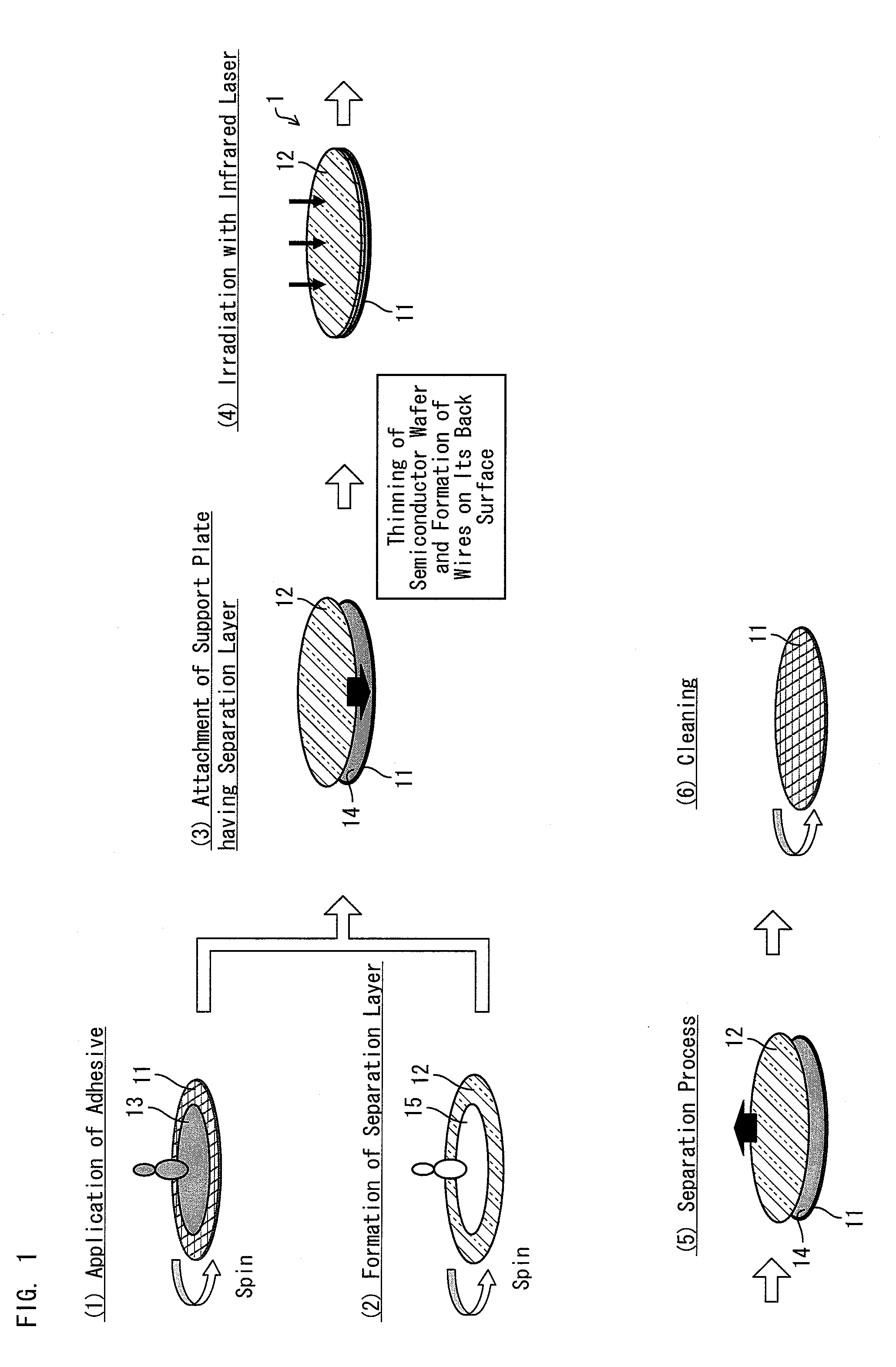
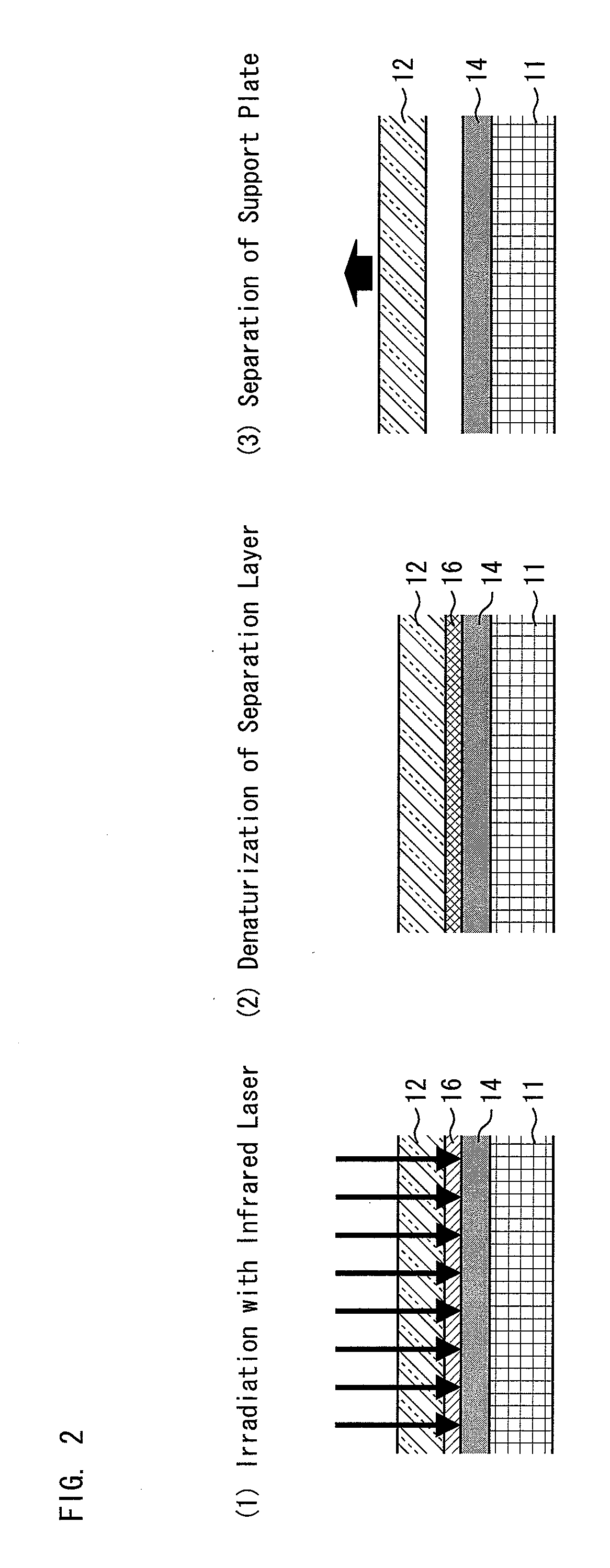
[0090]A laminate in Example 1 was prepared as follows. A tert-butylstyrene (TBST)-dimethylsiloxane copolymer having a siloxane structure, which is a copolymer of a repeating unit represented by Formula (3) below and a repeating unit represented by Formula (1) below (this copolymer is hereinafter referred to as Resin 1), was dissolved in PGMEA in such a manner that the content of the Resin 1 after dissolution was 20 weight %. Thus, a separation layer solution was obtained. An abundance ratio (molar ratio) of the repeating units in the Resin 1 was such that Formula (3): Formula (1)=1: 1. Weight-average molecular weight Mw of the Resin 1 was 8,000.

[0091]The separation layer solution was spin-applied onto a silicon wafer serving as a support plate in such a manner that the separation layer would have a thickness of 1 μm after baking the silicon wafer. Subsequently, the silicon wafer was heated in a stepwise manner for 1 min at 100° C., 160° C. and 220° C. so tha...


PUM

PropertyMeasurementUnit
Wavelengthaaaaaaaaaa
Fractionaaaaaaaaaa
Fractionaaaaaaaaaa

Abstract

A laminate including a supporter which transmits infrared; a substrate supported by the supporter; an adhesive layer via which the supporter and the substrate are attached to each other; and a separation layer, positioned on a surface of the supporter to which surface the substrate is attached, and made of a compound having an infrared-absorbing structure.

Description

[0001]This application claims priority under 35 U.S.C. §119(a)-(e) to Japanese Patent Application No. 2010-255349, filed on Nov. 15, 2010, and Japanese Patent Application No. 2011-229212, filed on Oct. 18, 2011, the entire contents of which are incorporated herein by reference.TECHNICAL FIELD[0002]The present invention relates to a laminate in which a supporter is temporarily attached to a product in production via a separation layer, and a method for separating the laminate.BACKGROUND ART[0003]Since mobile phones, digital AV devices, IC cards etc. are having more and more advanced functions, semiconductor silicon chips (hereinafter chips) mounted thereon are getting smaller and thinner. Consequently, there is an increasing demand for large-scale integration of silicon in a package. For example, integrated circuits in which a plurality of chips are one-packaged, such as CSP (Chip Size Package) and MCP (Multi-chip Package), are required to be thin. In order to realize large-scale int...

Claims


Application Information

Patent Timeline
IPC IPC(8): B32B38/10B32B7/06B32B9/04
CPCB32B38/10B32B2310/0825B32B2457/14H01L21/6835H01L2221/68327Y10T156/1195B32B43/006H01L2221/68318C08G77/14Y10T156/1158H01L2221/68381Y10T428/31663
Inventor IMAI, HIROFUMITAMURA, KOKIKUBO, ATSUSHIYOSHIOKA, TAKAHIROFUJII, YASUSHIINAO, YOSHIHIRO
Owner TOKYO OHKA KOGYO CO LTD
Why Eureka
Try Eureka