Conductive sheet, method for using conductive sheet, and capacitive touch panel

a capacitive touch panel and conductive sheet technology, applied in the direction of conductive layers on insulating supports, cables/conductor manufacture, instruments, etc., can solve the disadvantages of poor finger position detection accuracy, significantly deteriorating visibility, and described capacitive input devices, so as to improve visibility, reduce resistance of conductive pattern formed on the substrate, reduce the effect of resistan

Active Publication Date: 2012-05-17
FUJIFILM CORP
View PDF3 Cites 63 Cited by
  • Summary
  • Abstract
  • Description
  • Claims
  • Application Information

AI Technical Summary

Benefits of technology

[0003]However, the capacitive input device described in Japanese Laid-Open Patent Publication No. 2008-310551 is disadvantageously poor in finger position detection accuracy because it is necessary to form gaps between first and second electrode arrays arranged on one main surface of a substrate to prevent short circuit of the first and second electrode arrays. Furthermore, the capacitive input device is disadvantageous in that electrode connections of the second electrode arrays are formed on electrode connections of the first electrode arrays with insulation layers in between to prevent short circuit of intersections (cross points) of the first and second electrode arrays, whereby the intersections have large thicknesses and appear as local black points in the touch panel surface to significantly deteriorate the visibility. In addition, mask patterns are required to form the insulation layers and the electrode connections thereon, thereby resulting in complicated production process and high production cost.
[0007]In view of the above problems, an object of the present invention is to provide a conductive sheet and a conductive sheet using method, where the conductive sheet can have a low-resistance conductive pattern on a substrate, can exhibit an improved visibility, and can be suitably used in a projected capacitive touch panel or the like.
[0008]Another object of the present invention is to provide a touch panel that can have a low-resistance conductive pattern on a substrate, can exhibit an improved visibility, and can be suitably used as a large-sized projected capacitive touch panel or the like.
[0041]As described above, in the conductive sheet and the conductive sheet using method of the present invention, the resistance of the conductive pattern formed on the substrate can be lowered, the visibility can be improved, and the conductive sheet can be suitably used in a projected capacitive touch panel or the like.
[0042]Furthermore, in the touch panel of the present invention, the resistance of the conductive pattern formed on the substrate can be lowered, the visibility can be improved, and the touch panel can be suitably used as a large-sized projected capacitive touch panel or the like.

Problems solved by technology

However, the capacitive input device described in Japanese Laid-Open Patent Publication No. 2008-310551 is disadvantageously poor in finger position detection accuracy because it is necessary to form gaps between first and second electrode arrays arranged on one main surface of a substrate to prevent short circuit of the first and second electrode arrays.
Furthermore, the capacitive input device is disadvantageous in that electrode connections of the second electrode arrays are formed on electrode connections of the first electrode arrays with insulation layers in between to prevent short circuit of intersections (cross points) of the first and second electrode arrays, whereby the intersections have large thicknesses and appear as local black points in the touch panel surface to significantly deteriorate the visibility.
In addition, mask patterns are required to form the insulation layers and the electrode connections thereon, thereby resulting in complicated production process and high production cost.
However, this structure may cause the following problem in the future.
Thus, when the touch panel is used in the large devices in the above future trend, the large-sized touch panel exhibits a low current transfer rate between the electrodes, and thereby exhibits a low response speed (a long time between finger contact and touch position detection).

Method used


Image

  • Conductive sheet, method for using conductive sheet, and capacitive touch panel
  • Conductive sheet, method for using conductive sheet, and capacitive touch panel
  • Conductive sheet, method for using conductive sheet, and capacitive touch panel

Examples


examples

[0195]The present invention will be described more specifically below with reference to Examples. Materials, amounts, ratios, treatment contents, treatment procedures, and the like, used in Examples, may be appropriately changed without departing from the scope of the present invention.

[0196]The following specific Examples are therefore to be considered in all respects as illustrative and not restrictive.

first example

[0197]Conductive sheets of Comparative Examples 1 and 2 and Examples 1 to 6 were subjected to surface resistance and transmittance measurement and moire and visibility evaluation. The components, measurement results, and evaluation results of Comparative Examples 1 and 2 and Examples 1 to 6 are shown in Table 3.

example 1

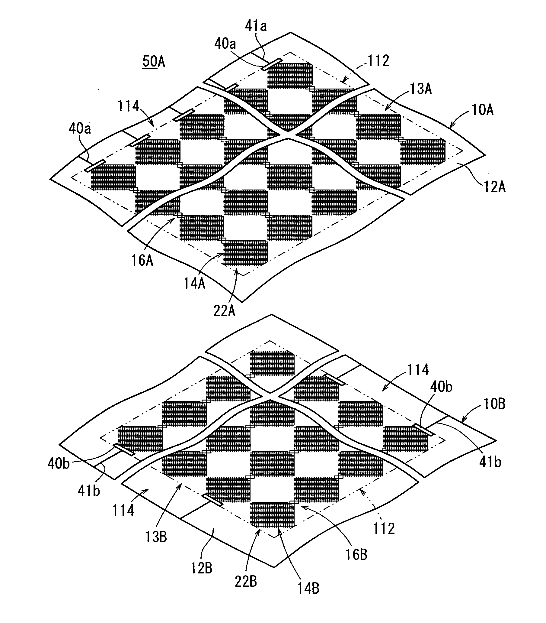
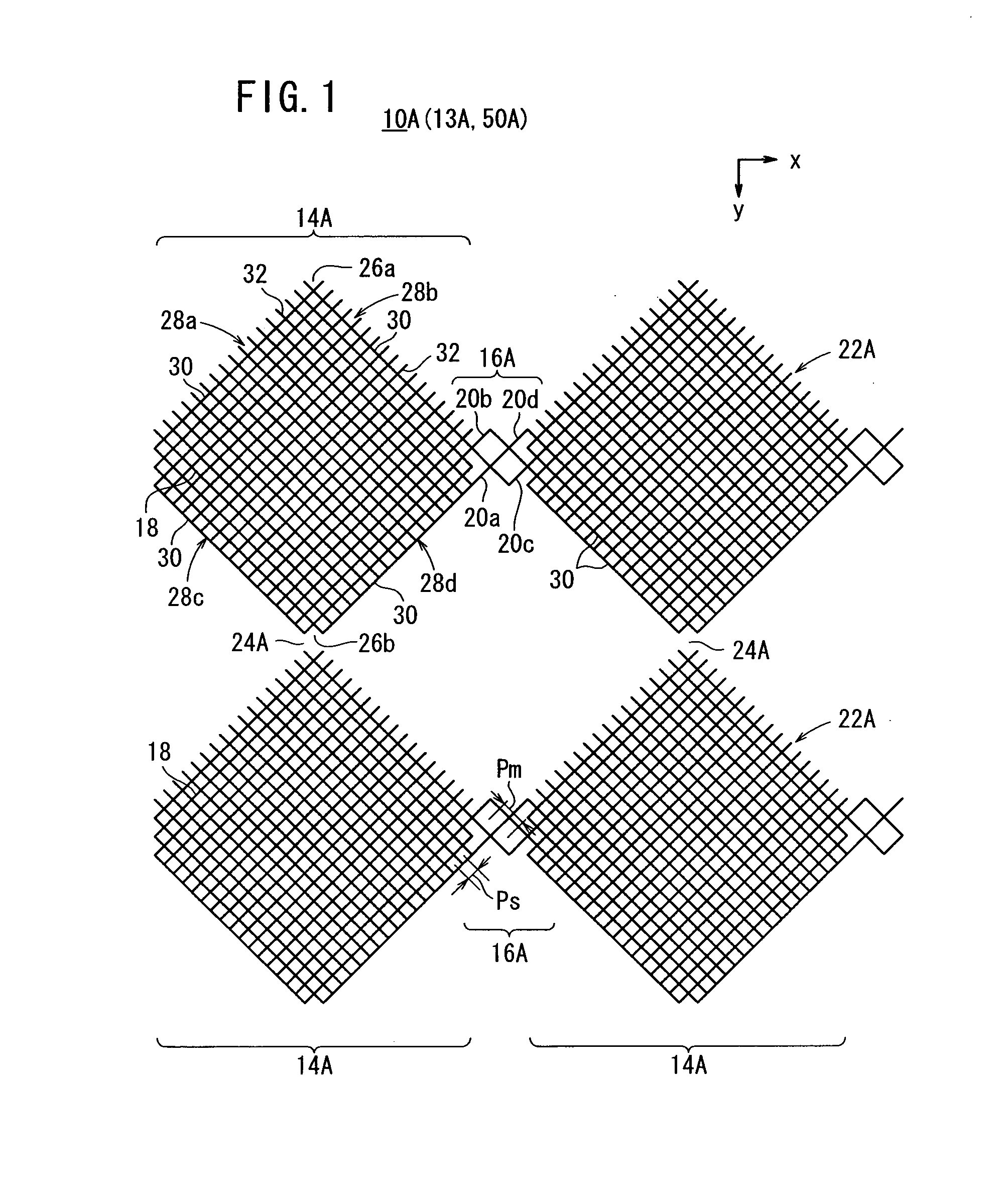
[0205]In the first conductive sheet 10A and the second conductive sheet 10B produced in example 1, the conductive portions (the first conductive patterns 22A and the second conductive pattern 22B) had a line width of 1 μm, the small lattices 18 had a side length of 50 μm, and the large lattices (the first large lattices 14A and the second large lattices 14B) had a side length of 3 mm.


PUM


Abstract

A conductive Sheet, a method for using conductive sheet, and a capacitive touch panel are provided. A first conductive sheet contains two or more conductive first large lattices and a first connection for electrically connecting the adjacent first large lattices on a first transparent substrate. The first large lattices each contain a combination of two or more small lattices, the first connection contains one or more medium lattices (a first medium lattice to a fourth medium lattice), and the pitch of the medium lattices is n times larger than that of the small lattices (in which n is a real number larger than 1).

Description

TECHNICAL FIELD[0001]The present invention relates to a conductive sheet, a method for using a conductive sheet, and a capacitive touch panel, and for example to a conductive sheet suitable for use in a projected capacitive touch panel, a method for using a conductive sheet, and a capacitive touch panel.BACKGROUND ART[0002]Common capacitive touch panels are position input devices capable of detecting a human finger touch position based on an electrostatic capacitance change between the finger and a conductive film. Such capacitive touch panels include surface capacitive touch panels and projected capacitive touch panels. The surface capacitive touch panel has a simple structure but is incapable of simultaneously detecting two or more touch points (multi-touch detection). On the other hand, the projected capacitive touch panel has a structure containing a large number of electrodes arranged in a matrix, similar to a pixel structure of a liquid crystal display device, etc. More specif...

Claims


Application Information

Patent Timeline
Patent Type & Authority Applications(United States)
IPC IPC(8): H05K1/02
CPCG06F3/044G06F2203/04111G06F2203/04112G06F3/0412G06F3/0445G06F3/0446H01B5/14H01B13/00
Inventor KURIKI, TADASHI
Owner FUJIFILM CORP
Why Eureka
Try Eureka