Crosstalk reduction between signal layers in a multilayered package by variable-width mesh plane structures

a multi-layer package and mesh plane technology, applied in the direction of printed circuit manufacturing, printed circuit aspects, conductive pattern formation, etc., can solve the problems of limiting signaling rate and performance, compromising the integrity of received data, and compromising the performance of the module, so as to reduce crosstalk interference, increase the likelihood, and increase the likelihood of containing the electromagnetic field associated

Inactive Publication Date: 2012-05-24
IBM CORP
View PDF30 Cites 15 Cited by
  • Summary
  • Abstract
  • Description
  • Claims
  • Application Information

AI Technical Summary

Benefits of technology

[0010]An embodiment of the invention provides a mesh wire structure for mesh planes with mesh wiring of varying widths for reducing crosstalk interference experienced in signal lines due to the inductive effects from signals in one plane interacting with signals in other signal planes of a multilayer ceramic package. A first selection of mesh line segments of a mesh layer are of a first width and a second selection of mesh line segments of the mesh layer are of a second width, wherein the second width is greater than the first width. The second selection of mesh line segments of the second width are positioned in parallel to a selection of signal lines in a signal layer that are likely to introduce crosstalk, wherein the widening of the mesh line segmen

Problems solved by technology

In addition, with vias establishing electrical connections between layers, if a mesh line runs too close to a via, yield detracting shorts may be introduced which compromise the performance of the module, therefore via clearances set the minimum distance between

Method used


Image

  • Crosstalk reduction between signal layers in a multilayered package by variable-width mesh plane structures
  • Crosstalk reduction between signal layers in a multilayered package by variable-width mesh plane structures
  • Crosstalk reduction between signal layers in a multilayered package by variable-width mesh plane structures

Examples


Embodiment Construction

[0021]In the following description, for the purposes of explanation, numerous specific details are set forth in order to provide a thorough understanding of the present invention. It will be apparent, however, to one skilled in the art that the present invention may be practiced without these specific details. In other instances, well-known structures and devices are shown in block diagram form in order to avoid unnecessarily obscuring the present invention.

[0022]In addition, in the following description, for purposes of explanation, numerous systems are described. It is important to note, and it will be apparent to one skilled in the art that the present invention may execute in a variety of systems, including a variety of computer systems and electronic devices operating any number of different types of operating systems.

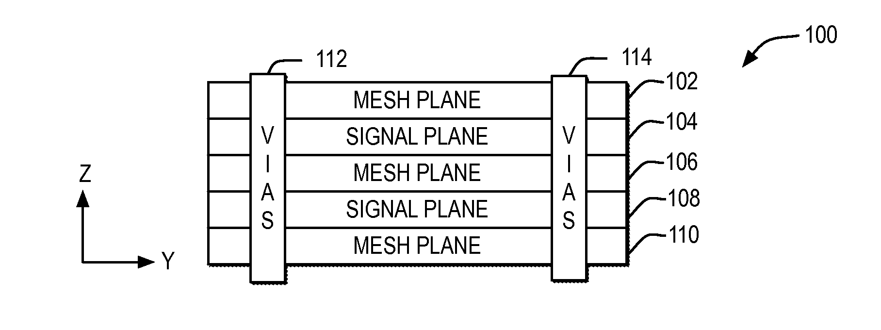
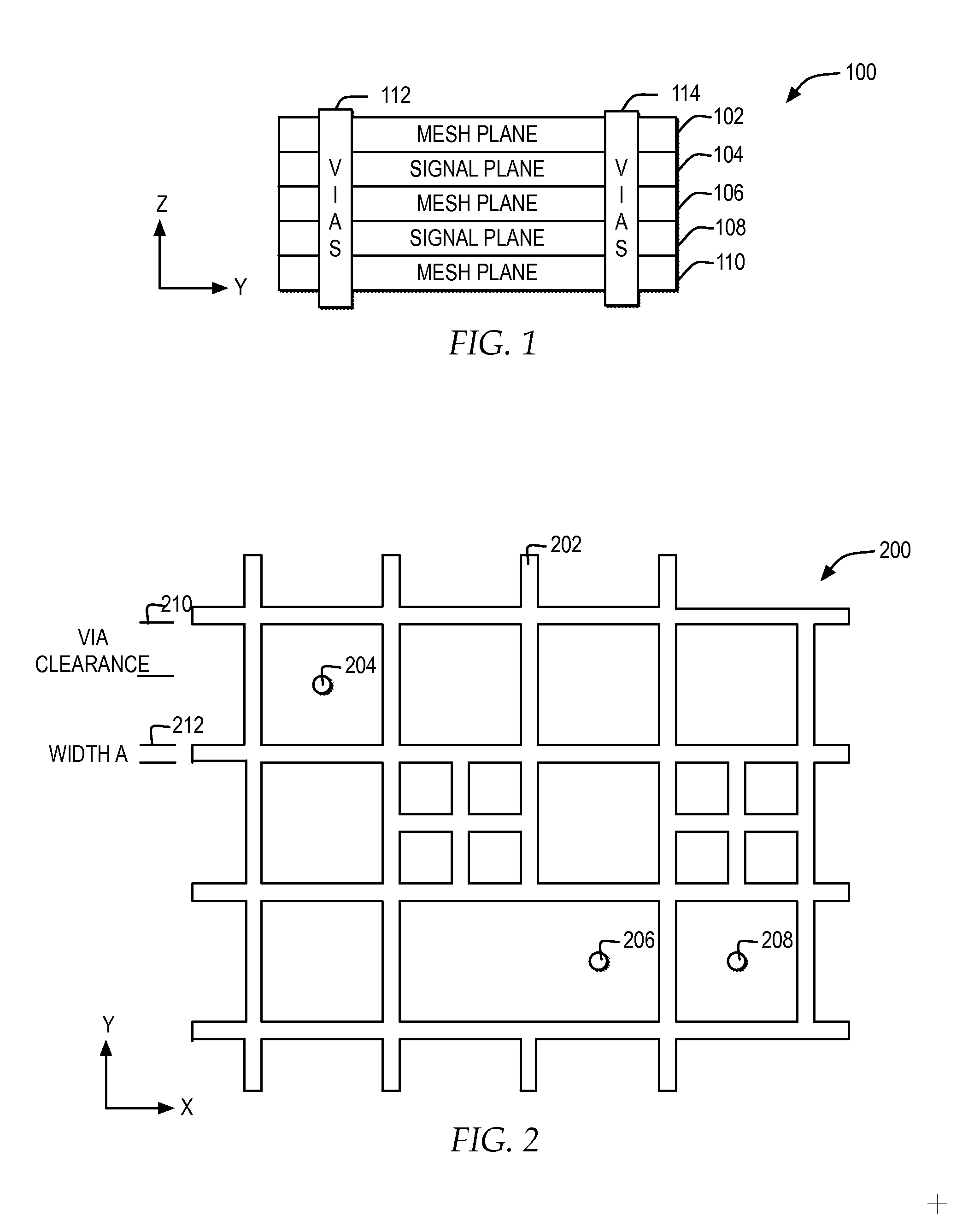
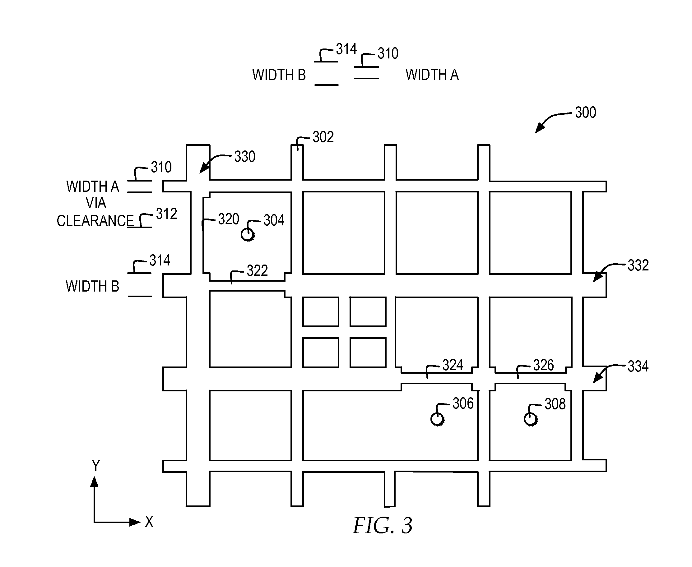
[0023]FIG. 1 illustrates a side view of examples of layers of a multilayer ceramic (MLC) package with multiple mesh planes, signal planes, and vias interconnectin...


PUM

PropertyMeasurementUnit
Mesh sizeaaaaaaaaaa
Diameteraaaaaaaaaa
Widthaaaaaaaaaa

Abstract

A first selection of mesh line segments of a mesh layer are of a first width and a second selection of mesh line segments of the mesh layer are of a second width, wherein the second width is greater than the first width. The second selection of mesh line segments of the second width are positioned in parallel to a selection of signal lines in a signal layer that are likely to introduce crosstalk, wherein the widening of the mesh line segments shadowing the selection of signal lines increases the likelihood that the return current associated with the signal will flow in the wider mesh line segment, thereby increasing the likelihood of containing the electromagnetic fields associated with the signal such that crosstalk to other signals is reduced or contained.

Description

BACKGROUND[0001]1. Technical. Field[0002]The invention relates generally to an improved apparatus and method for crosstalk reduction in a multilayered package and more specifically, the invention is directed to an apparatus and method for crosstalk reduction in multilayered ceramic packages using variable-width mesh structures.[0003]2. Description of Related Art[0004]Multilayer modules are used for the packaging of electronic components, and in particular, for packaging integrated circuit chips. Both single chip modules (SCM) and multi chip modules (MCM) are widely used. One common type of chip module is the multilayer ceramic packaging module. In a multilayer ceramic packaging module, multiple layers consist of ceramic or glass-ceramic material, for example.[0005]In one example, a multilayer ceramic fabrication process involves the formation of green or unfired ceramic layers or sheets, the formation of conductive paste, the screening of the conductive paste onto the green ceramic ...

Claims


Application Information

Patent Timeline
IPC IPC(8): H05K1/11H05K3/10
CPCH05K1/0224H05K1/116H05K2201/09681H05K2201/09718Y10T29/49155H05K1/0228H05K3/46Y10T29/53022Y10T29/49004H05K2201/09727G06F30/398
Inventor CHOI, JINWOOCHUN, SUNGJUNFRANKEL, JASON L.WALLING, PAUL R.WEEKLY, ROGER D.
Owner IBM CORP
Why Eureka
Try Eureka