Liquid Crystal Display Device and Method for Manufacturing the Same

a liquid crystal display device and liquid crystal technology, applied in liquid surface applicators, instruments, coatings, etc., can solve the problems of complex manufacturing process steps and increased manufacturing costs, and achieve the effect of reducing manufacturing costs, simplifying manufacturing process steps, and reducing overall thickness of liquid crystal display devices

Active Publication Date: 2012-05-24
LG DISPLAY CO LTD
View PDF4 Cites 44 Cited by
  • Summary
  • Abstract
  • Description
  • Claims
  • Application Information

AI Technical Summary

Benefits of technology

[0016]An advantage of the present invention is to provide a liquid crystal display device and a method for manufacturing the same, in which a sensing electrode for sensing a touch of a user is built in a liquid crystal panel so as not to require a separate touch screen on the liquid crystal panel, whereby the overall thickness of the liquid crystal display device is reduced, manufacturing process steps are simplified, and the manufacturing cost is reduced.
[0017]Additional advantages and features of the invention will be set forth in part in the description which follows and in part will become apparent to those having ordinary skill in the art upon examination of the following or may be learned from practice of the invention. The objectives and other advantages of the invention may be realized and attained by the structure particularly pointed out in the written description and claims hereof as well as the appended drawings.
[0018]To achieve these objects and other advantages and in accordance with the purpose of the invention, as embodied and broadly described herein, a liquid crystal display device comprises gate and data lines arranged to cross each other on a substrate to define a plurality of pixels; a pixel electrode formed in each of the plurality of pixels; a common electrode forming an electric field together with the pixel electrode, patterned to sense a touch of a user; a sensing line discontinuously formed on the common electrode and electrically connected with the common electrode; a jump line formed below the common electrode to electrically connect discontinuous portions of the sensing line with one another; and first and second connection electrodes for electrically connecting the jump line with the sensing line, wherein the first connection electrode is connected with the jump line, and the second connection electrode is connected with the sensing line and the first connection electrode respectively.
[0019]In another aspect of the present invention, a method for manufacturing a liquid crystal display device comprises the steps of patterning a jump line on a substrate; forming an interlayer insulating film on the jump line; forming a first contact hole in the interlayer insulating film to expose the jump line; forming a first connection electrode connected with the jump line through the first contact hole; forming a first passivation film by sequentially depositing an inorganic film and an organic film on the first connection electrode; forming an opening in the organic film of the first passivation film; patterning a common electrode on the organic film of the first passivation film and patterning a sensing line on the common electrode; forming a second passivation film on the sensing line; forming a second contact hole to expose the sensing line and the first connection electrode by removing a predetermined region of the second passivation film and a predetermined region of the inorganic film of the first passivation film; and forming a second connection electrode connected with the sensing line and the first connection electrode through the second contact hole.

Problems solved by technology

For this reason, problems occur in that manufacturing process steps are complicated and the manufacturing cost is increased.

Method used


Image

  • Liquid Crystal Display Device and Method for Manufacturing the Same
  • Liquid Crystal Display Device and Method for Manufacturing the Same
  • Liquid Crystal Display Device and Method for Manufacturing the Same

Examples


Embodiment Construction

[0029]Reference will now be made in detail to the exemplary embodiments of the present invention, examples of which are illustrated in the accompanying drawings. Wherever possible, the same reference numbers will be used throughout the drawings to refer to the same or like parts.

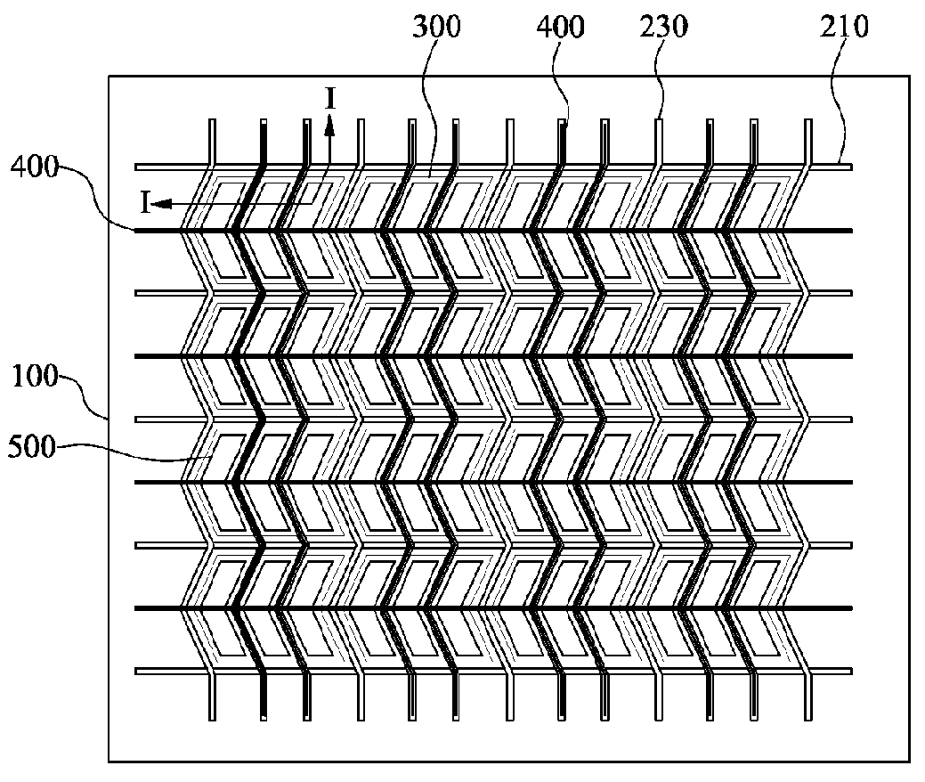
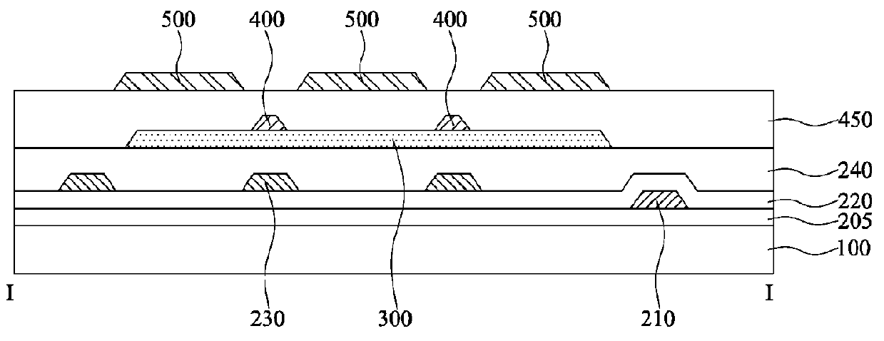
[0030]FIG. 2a is a plane view illustrating a lower substrate for a liquid crystal display device according to one embodiment of the present invention, and FIG. 2b is a cross-sectional view taken along line I-I of FIG. 2a.

[0031]As shown in FIG. 2a, the liquid crystal display device according to one embodiment of the present invention includes a substrate 100, a gate line 210, a data line 230, a common electrode 300, a sensing line 400, and a pixel electrode 500.

[0032]The substrate 100 may be formed of glass or transparent plastic.

[0033]The gate line 210 is arranged on the substrate 100 in a horizontal direction, and the data line 230 is arranged on the substrate 100 in a vertical direction. In this way, the ...


PUM

PropertyMeasurementUnit
electric fieldaaaaaaaaaa
electricallyaaaaaaaaaa
light transmittanceaaaaaaaaaa

Abstract

A liquid crystal display device and a method for manufacturing the same are disclosed. The liquid crystal display device comprises gate and data lines arranged to cross each other on a substrate to define a plurality of pixels; a pixel electrode formed in each of the plurality of pixels; a common electrode forming an electric field together with the pixel electrode, patterned to sense a touch of a user; a sensing line discontinuously formed on the common electrode and electrically connected with the common electrode; a jump line formed below the common electrode to electrically connect discontinuous portions of the sensing line with one another; and first and second connection electrodes for electrically connecting the jump line with the sensing line, wherein the first connection electrode is connected with the jump line, and the second connection electrode is connected with the sensing line and the first connection electrode respectively.

Description

CROSS REFERENCE TO RELATED APPLICATIONS[0001]This application claims the benefit of the Korean Patent Application No. 10-2010-0116166 filed on Nov. 22, 2010, which is hereby incorporated by reference for all purposes as if fully set forth herein.BACKGROUND OF THE INVENTION[0002]1. Field of the Invention[0003]The present invention relates to a liquid crystal display device, and more particularly, to a liquid crystal display device provided with a sensing electrode for sensing a touch of a user.[0004]2. Discussion of the Related Art[0005]A liquid crystal display device is widely used in various fields of notebook computers, monitors, spacecraft, aircraft, and etc. owing to advantages of low power consumption based on a low driving voltage and portability.[0006]The liquid crystal display device includes a lower substrate, an upper substrate, and a liquid crystal layer formed between the lower and upper substrates. In the liquid crystal display device, an alignment state of liquid cryst...

Claims


Application Information

Patent Timeline
Patent Type & Authority Applications(United States)
IPC IPC(8): G02F1/1343B05D5/12
CPCG06F3/0412G06F3/044G06F2203/04111G02F2001/134372G09G2300/0426G02F1/13338G02F1/136227G09G3/3648G06F3/0443G06F3/0446G02F1/134372
Inventor SHIN, HEESUN
Owner LG DISPLAY CO LTD
Why Eureka
Try Eureka