

Resin multilayer substrate and method for manufacturing the resin multilayer substrate
a multi-layer substrate and resin technology, applied in the direction of sustainable manufacturing/processing, final product manufacturing, semiconductor/solid-state device details, etc., can solve the problems of not being able to increase the density of conductive paste in the blind, reduce the resistance value, and reduce the possibility of peeling off
- Summary
- Abstract
- Description
- Claims
- Application Information
AI Technical Summary
Benefits of technology
Problems solved by technology
Method used
Image

Examples
embodiment 1
Preferred Embodiment 1
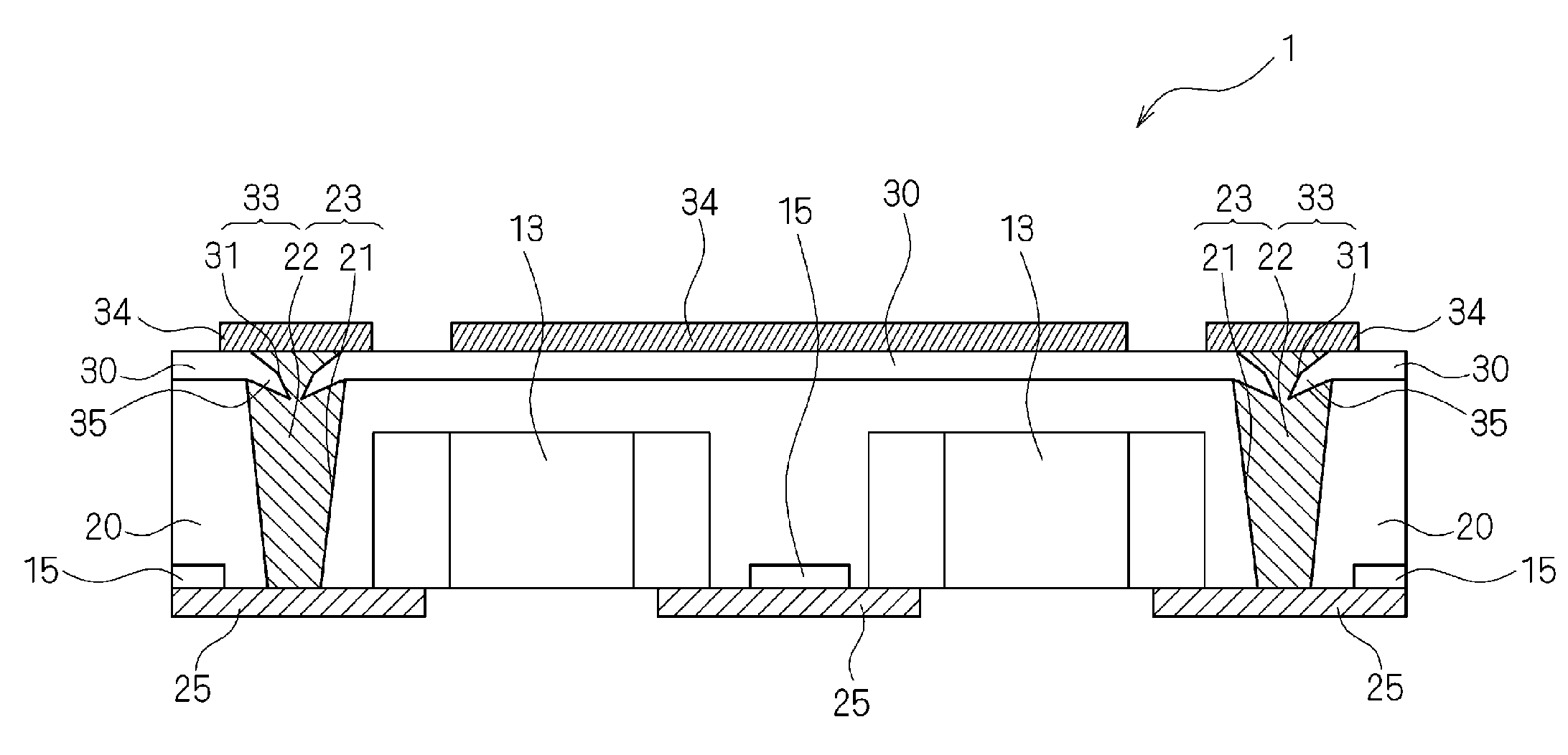
[0045]FIG. 1 is a schematic diagram illustrating the structure of a resin multilayer substrate according to preferred embodiment 1 of the present invention. As shown in FIG. 1, the resin multilayer substrate 1 according to preferred embodiment 1 includes a base layer 10, a component-containing layer (a first resin layer) 20, and a thin resin layer (a second resin layer) 30 which are stacked sequentially. The base layer 10 preferably is made of a ceramic, glass, an epoxy resin, or other suitable material, which has wiring patterns 11a, 11b located on both sides. The surface of the base layer 10 including the wiring pattern 11a and the surface thereof including the wiring pattern 11b respectively have an IC element 12 and a plurality of electronic components 13 mounted thereon preferably through a conductive joining material (not shown) such as solder. The plurality of electronic components 13 preferably are surface-mounted components, which are, for example, chi...
embodiment 2
Preferred Embodiment 2
[0063]FIGS. 14 and 15 are schematic diagrams for explaining a method for manufacturing a resin multilayer substrate 1 according to preferred embodiment 2 of the present invention. FIG. 14 shows pressurizing, in a direction toward a thin resin layer 30, metal foil 40 attached to the thin resin layer 30 after via holes 21, 31 in communication with each other are filled with a conductive paste 22, and FIG. 15 shows the metal foil 40 subjected to pressurization in the direction toward the thin resin layer 30. The method for manufacturing the resin multilayer substrate 1 according to preferred embodiment 2 preferably is the same or substantially the same as the manufacturing method according to Preferred embodiment 1 as shown in FIGS. 2 through 8, except that the thin resin layer 30 itself is stacked on a component-containing layer 20 without attaching a retention film 38 to the thin resin layer 30, and detailed descriptions will be thus omitted. It is to be noted t...
embodiment 3
Preferred Embodiment 3
[0066]FIG. 16 is a schematic diagram illustrating the structure of via holes 21, 31 in a resin multilayer substrate 1 according to preferred embodiment 3 of the present invention. It is to be noted that while FIG. 16 illustrates via conductors 23, in communication with each other included in a resin multilayer substrate 1 and the vicinity of the via conductors, the other structure preferably is the same or substantially the same as the structure of the resin multilayer substrate 1 shown in FIG. 1, and the illustration of the structure is thus omitted. It is to be noted that while FIG. 16 shows an example of changing the taper angle of a via hole 21 in stages for the purpose of illustration, the taper angle of a via hole 21 is continuously changed in the case of an actual resin-layered substrate 1. It is to be noted that the taper angle refers to an angle formed by a perpendicular line relative to the surface of a base layer 10 with a wiring pattern 11b located ...
PUM
| Property | Measurement | Unit |
|---|---|---|
| Angle | aaaaa | aaaaa |
| Electrical conductor | aaaaa | aaaaa |
Abstract
Description
Claims
Application Information