

Semiconductor device
- Summary
- Abstract
- Description
- Claims
- Application Information
AI Technical Summary
Benefits of technology
Problems solved by technology
Method used
Image

Examples
embodiment mode 1
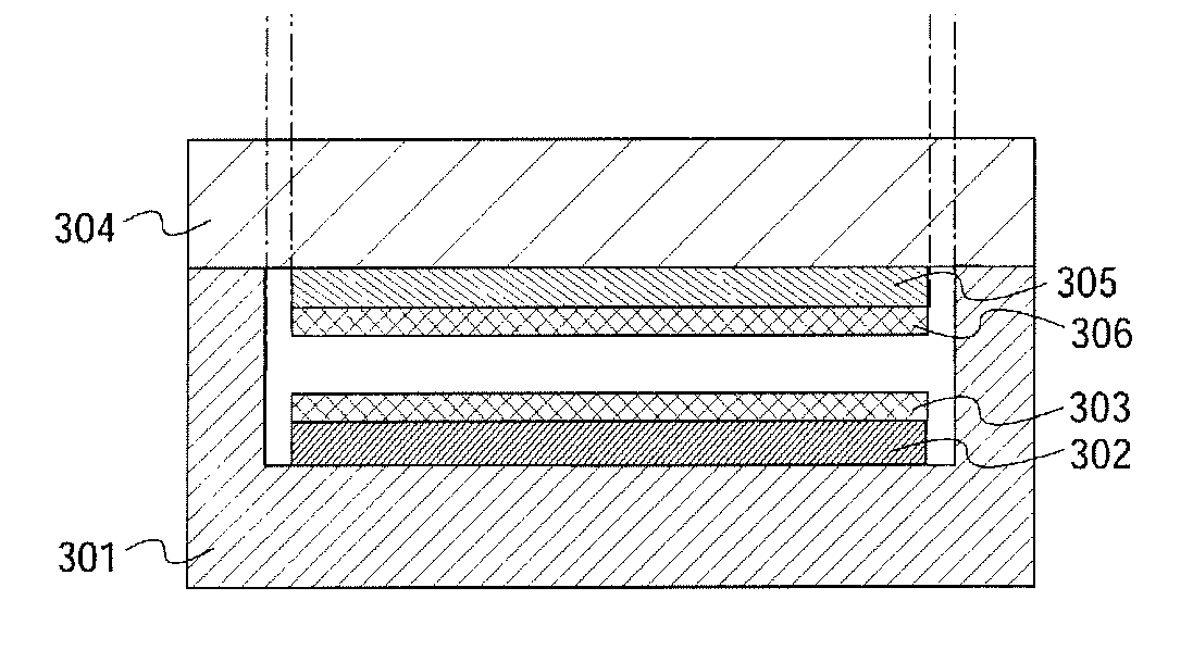
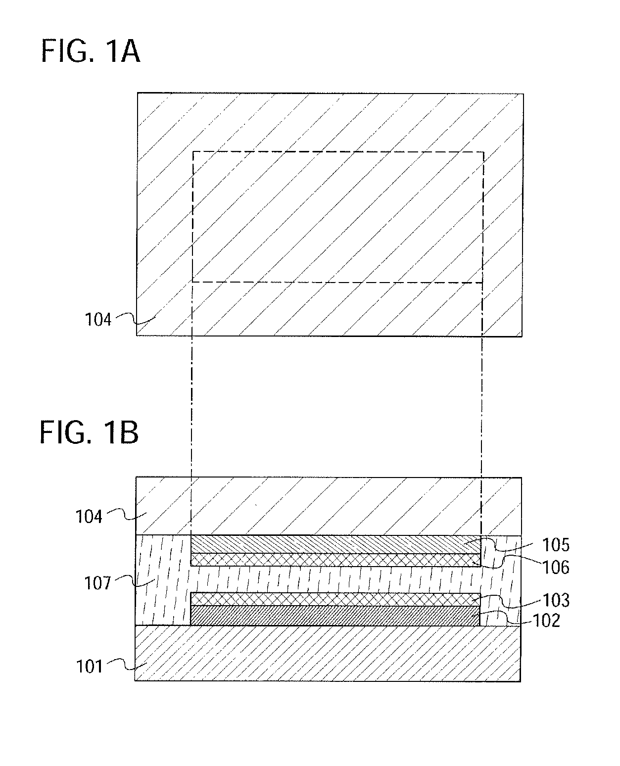
[0048]Examples of a semiconductor device of the present invention are described with reference to FIGS. 1A to 3E. FIGS. 1A and 1B are conceptual diagrams showing one mode of a semiconductor device of this embodiment mode. FIG. 1A is a top view and FIG. 1B is a cross-sectional view.
[0049]A first element group 102 and a first antenna 103 are provided over a first substrate 101. The first antenna 103 is connected to the first element group 102 physically and electrically. A second element group 105 and a second antenna 106 are provided on a second substrate 104. The second antenna 106 is connected to the second element group 105 physically and electrically.
[0050]Note that in this embodiment mode, an electronic circuit having a semiconductor element provided over a first substrate is referred to as a first element group, and an electronic circuit having a semiconductor element provided on a second substrate, a transducer, or the like is referred to as a second element group for convenie...
embodiment mode 2
[0079]An example of an embodiment mode of the present invention is described with reference to FIGS. 4A and 4B. FIGS. 4A and 4B each show a conceptual cross-sectional view of one mode of a semiconductor device of this embodiment mode. Note that structures of elements groups, antennas, and the like are similar to those of Embodiment Mode 1.
[0080]In the semiconductor device shown in FIG. 4A, the surface of the first substrate 101 and the rear surface of the second substrate 104 are bonded to each other with the bonding layer 107 interposed therebetween. In the semiconductor device shown in FIG. 4B, the rear surface of the first substrate 101 and the rear surface of the second substrate 104 are bonded to each other with the bonding layer 107 interposed therebetween.
[0081]Note that a surface of a substrate corresponds to a surface on which an element group is provided, and a rear surface of a substrate corresponds to a surface on which an element group is not provided.
[0082]In the semic...
embodiment mode 3
[0085]An example of an embodiment mode of the present invention is described with reference to FIGS. 5A and 7B. FIGS. 5A and 5B show one mode of a semiconductor device of this embodiment mode. Note that structures of elements groups, antennas, and the like are similar to those of Embodiment Mode 1.
[0086]FIGS. 5A and 5B show the semiconductor device of this embodiment mode. FIG. 5A is a top view and FIG. 5B is a cross-sectional view. In the semiconductor device shown in FIGS. 5A and 5B, a surface of a first substrate 201 and a surface of a second substrate 204 are bonded to each other with a bonding layer 207 interposed therebetween. Unlike the semiconductor device shown in FIGS. 1A and 1B, the bonding layer 207 is not provided over the entire surface of the substrate but is provided on only part of the substrate. Specifically, the bonding layer 207 is provided in a region which does not overlap with a first element group 202 provided over the first substrate 201 and a second element...
PUM
 Abstract
Description
Claims
Application Information