Flexible printed wiring substrate

a flexible, printed substrate technology, applied in the direction of printed circuit manufacturing, printed circuit aspects, high frequency circuit adaptations, etc., can solve the problem that the single flexible substrate cannot connect all the wires, and achieve the effect of reducing the occurrence of electrode displacement, high reliability, and advanced downsizing and high-density packaging of optical transmission modules

Active Publication Date: 2018-05-03
NTT ELECTORNICS CORP
View PDF0 Cites 1 Cited by
  • Summary
  • Abstract
  • Description
  • Claims
  • Application Information

AI Technical Summary

Benefits of technology

[0034]As described above, according to the flexible substrate having the branch structure in the present invention, it is possible to form a compact folded-up structure with high reliability in bodies of a branched flexible substrate, and further to reduce the occurrence of displacement of electrodes and a deformation or damage of the joint portion in a soldering process. The flexible substrate in the present invention is effective to advance downsizing and high-density packaging of optical transmission modules, and to prevent deterioration of high-frequency characteristics and a decrease in the yield of optical transmission modules.

Problems solved by technology

If the numbers of signal wires and power supply wires are increased, a situation may occur in which a single flexible substrate cannot connect all the wires.

Method used


Image

  • Flexible printed wiring substrate
  • Flexible printed wiring substrate
  • Flexible printed wiring substrate

Examples


embodiment 1

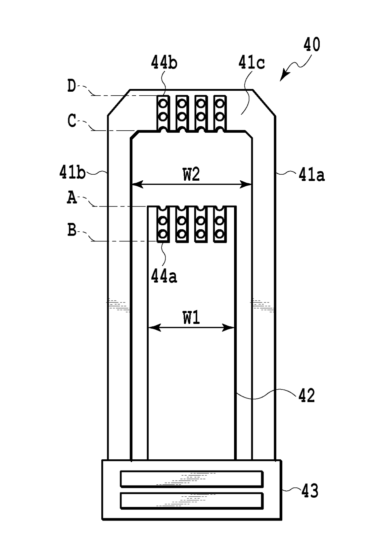
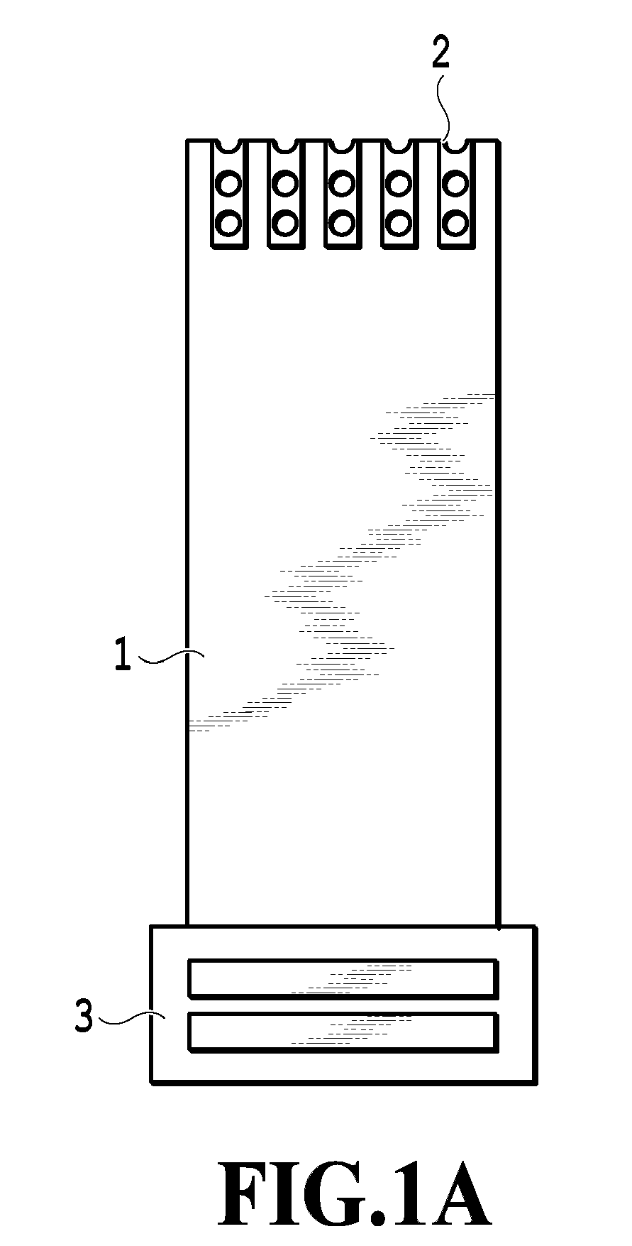
[0052]FIGS. 4A and 4B are views illustrating a structure of an unfolded state of a flexible substrate in Embodiment 1 of the present invention. FIG. 4A is a view of a side of the flexible substrate on which solder joint surfaces and pins of a connector are seen, whereas FIG. 4B is a view of the side opposite to FIG. 4A. A flexible substrate 40 includes a connector 43 at one end thereof, the connector 43 equipped with multiple pins for connection. A first body 42 and a second body of the flexible substrate are connected with the connector 43. The second body includes three side portions (41a, 41b, 41c) and is in a band-like form in an approximately squared-U or U shape, as will be described later. Both the first body 42 and the second body 41 are provided with a conductor foil formed using a film-form insulator as a base, as in the flexible substrates illustrated in FIGS. 1A and 2A. Although not illustrated in FIGS. 4A and 4B, the first body 42 and the second body 41 are joined to ea...

embodiment 2

[0066]FIGS. 7A and 7B are views illustrating structures of flexible substrates in Embodiment 2 of the present invention, and each present an unfolded state before folding-up. FIGS. 7A and 7B illustrate two different modification examples. The basic structure is the same as the structure of the flexible substrate in Embodiment 1 illustrated in FIGS. 4A and 4B, and only different points from those in Embodiment 1 are explained herein. A flexible substrate 70 in FIG. 7A illustrates a first modification example, and is different from the structure in Embodiment 1 only in the structure of a second body (71a and 71b). In Embodiment 1 illustrated in FIGS. 4A and 4B, the second body includes the two side portions 41a, 41b extending in parallel to the longitudinal direction of the whole flexible substrate, and the transverse side portion 41, and is formed in the closed band-like form to surround the periphery of the first body 42.

[0067]In Modification Example 1 in FIG. 7A, the second body (7...

embodiment 3

[0071]In the present embodiment, illustrated is a structural example in which the work in soldering the flexible substrates in aforementioned Embodiments of the present invention to optical transmission modules or the like is facilitated to be more efficiently carried out. In the flexible substrate in the present invention, the structure in which the second body is unsharply folded in the longitudinal direction of the whole flexible substrate significantly reduces the peel stress due to the stiffness of the folded portion in the soldering process of the two bodies. However, the soldering step of the second body involving reheating needs cautions on the work for minimizing the aforementioned stress. In the present embodiment, illustrated is the structural example that reduces the stress which is applied during the work in the soldering process due to variations in skill among workers.

[0072]FIGS. 8A and 8B are views for explaining a structure of a flexible substrate in Embodiment 3 of...


PUM


Abstract

A flexible substrate having a branch structure in the related art has problems in that: adhesive strength after two bodies are folded and fixed at a bonding region decreases due to an unfolding and opening force at a curve portion and ends of the bonded portions are peeled off and generate gaps; and in a soldering process of the two bodies, the electrodes of one body soldered first are displaced due to reheating in soldering the other body secondly and deteriorate in soldered connection. The present invention provides a new flexible substrate having a branch structure, including first and second bodies joined together, and having a structure in which one of the bodies can be folded back in a longitudinal direction of the whole flexible substrate. Tip ends of the two bodies are provided with multiple electrodes, and are connected by soldering to approximately corresponding positions on both surfaces of an end portion of a printed substrate concerned.

Description

TECHNICAL FIELD[0001]The present invention relates to a connection structure and a connection method for electrically connecting substrates on which electronic circuits, optical circuits and the like are mounted. More specifically, the present invention relates to a flexible printed wiring substrate which is made of a flexible material and which connects various circuit substrates.BACKGROUND ART[0002]As important components in the field of optical communication, optical transmission modules having basic functions such as electro-optic conversion, photoelectric conversion, amplification, reproduction, and modulation / demodulation are used in a wide range of applications. With the background of speed-up and a capacity increase of wired networks and wireless networks, the optical transmission modules are required to perform signal processing at higher speed, and are strongly required at the same time to achieve cost reduction and enhancement of reliability. The optical transmission modu...

Claims


Application Information

Patent Timeline
Patent Type & Authority Applications(United States)
IPC IPC(8): H05K1/14H05K1/02H05K1/11
CPCH05K1/147H05K1/028H05K1/0237H05K1/115H05K2201/09027H05K2201/10189H05K3/363H05K1/02
Inventor YOSHIDA, KAZUMASAOZAWA, TOSHIYUKISATO, TERUAKITOMITA, ATSUSHITAKEUCHI, YOSUKEMINO, SHINJINASU, YUSUKE
Owner NTT ELECTORNICS CORP
Why Eureka
Try Eureka