Photosensor, semiconductor device, and liquid crystal panel

a semiconductor device and photosensor technology, applied in semiconductor devices, radio frequency controlled devices, instruments, etc., can solve the problem of not providing sufficient light detection sensitivity, and achieve the effect of improving light detection sensitivity and light use efficiency

Inactive Publication Date: 2012-06-21
SHARP KK
View PDF3 Cites 15 Cited by
  • Summary
  • Abstract
  • Description
  • Claims
  • Application Information

AI Technical Summary

Benefits of technology

[0012]An object of the present invention is to solve this problem with the conventional art by improving light use efficiency and thus improving the light detection sensitivity of the thin film diode even when the semiconductor layer of the thin film diode has a small thickness.
[0014]According to the present invention, asperities are provided on the side of the silicon layer facing the first semiconductor layer, such that light that entered the silicon layer is emitted from the silicon layer in different directions. As a result, light from different directions enters the first semiconductor layer. Since asperities are provided on both sides of the first semiconductor layer in the thickness direction, light that entered the first semiconductor layer travels a longer distance inside the first semiconductor layer. As a result, more light is absorbed in the first semiconductor layer. Accordingly, light use efficiency and thus light detection sensitivity will be improved even with a first semiconductor layer with a small thickness.

Problems solved by technology

However, even the semiconductor device shown in FIG. 14 does not provide sufficient light detection sensitivity.

Method used


Image

  • Photosensor, semiconductor device, and liquid crystal panel
  • Photosensor, semiconductor device, and liquid crystal panel
  • Photosensor, semiconductor device, and liquid crystal panel

Examples


embodiment 1

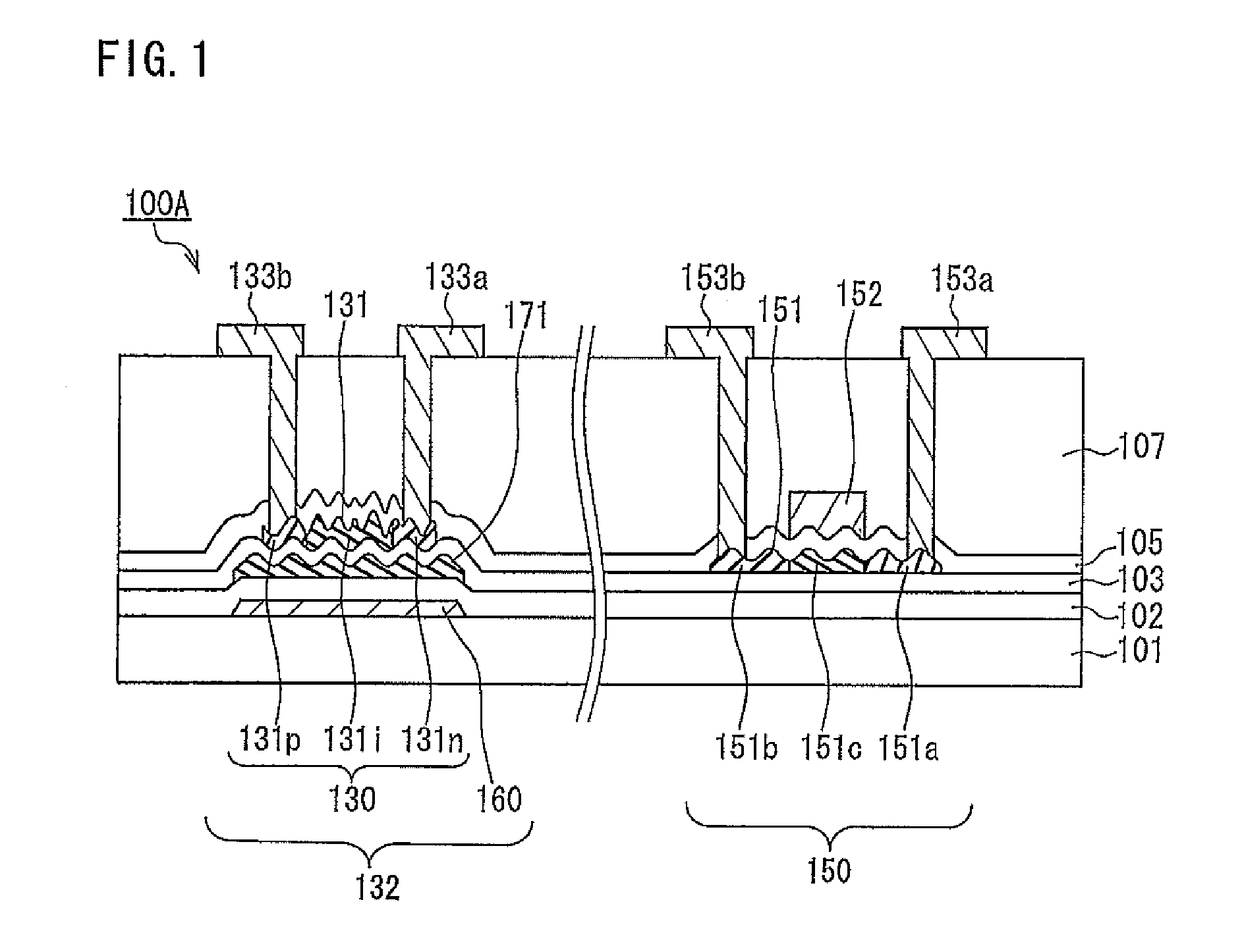
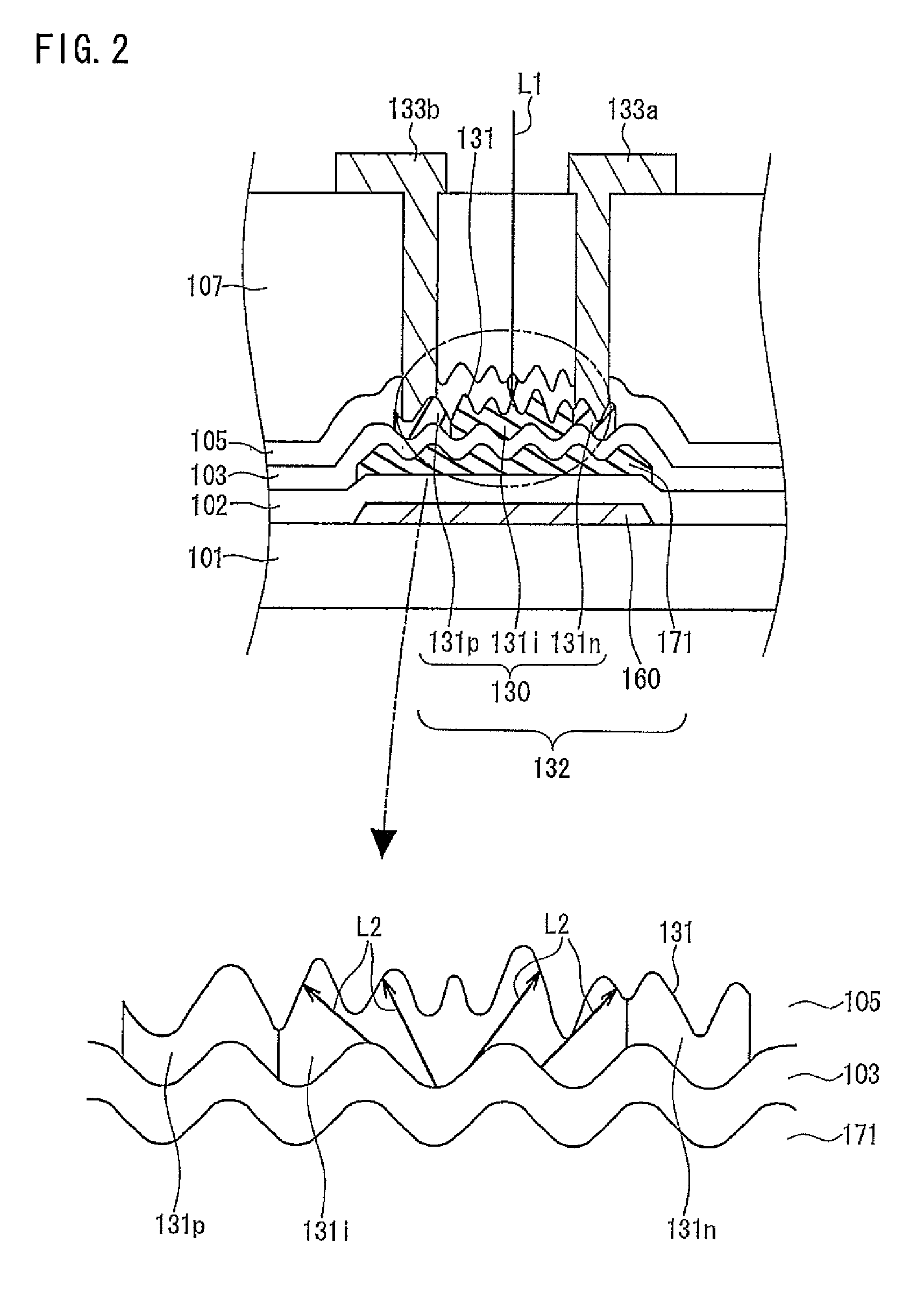
[0055]FIG. 1 is a schematic cross sectional view of a semiconductor device 100A according to Embodiment 1 of the present invention. The semiconductor device 100A includes: a photosensor 132 having a substrate 101, a thin film diode 130 formed above the substrate 101 with interposed base layers 102 and 103 therebetween as insulating layers, a polycrystalline silicon layer (silicon layer) 171 provided between the substrate 101 and the thin film diode 130, and a light-blocking layer 160 provided between the substrate 101 and the polycrystalline silicon layer 171; and a thin film transistor 150. The substrate 101 is preferably translucent. To simplify the drawing, FIG. 1 only shows a single photosensor 132 and a single thin film transistor 150; however, a plurality of photosensors 132 and a plurality of thin film transistors 150 may be formed on a common substrate. Further, to facilitate understanding, FIG. 1 shows a cross section of the photosensor 132 and that of the thin film transis...

embodiment 2

[0105]FIG. 4 is a schematic cross sectional view of a semiconductor device 100B according to Embodiment 2 of the present invention. In FIG. 4, the same components and locations as in the semiconductor device 100A of Embodiment 1 are labeled with the same numerals and their description will be omitted. A semiconductor device 100B of Embodiment 2 will now be described focusing on the differences between Embodiments 1 and 2.

[0106]In Embodiment 2, an n-type region 171n and a p-type region 171p are formed in the polycrystalline silicon layer 171, and an electrodes 133a and 133b are electrically connected with the n-type region 171n and the p-type region 171p, respectively. An intrinsic region 171i is provided between the n-type region 171n and the p-type region 171p.

[0107]In such a structure, the polycrystalline silicon layer 171 may function as a second thin film diode 170. Accordingly, a photosensor 134 including a double-structure thin film diode having a first thin film diode 130 an...

embodiment 3

[0117]FIG. 7 is a schematic cross sectional view of a semiconductor device 100C according to Embodiment 3 of the present invention. In FIG. 7, the same components and locations as in the semiconductor device 100B of Embodiment 2 are labeled with the same numerals and their description will be omitted. A semiconductor device 100C of Embodiment 3 will now be described focusing on the differences between Embodiments 2 and 3.

[0118]In Embodiment 3, a semiconductor layer (first semiconductor layer) 132 constituting the thin film diode 130 is made of amorphous silicon and thus it is different from the semiconductor layer 131 of Embodiment 2 made of a polycrystalline semiconductor (polycrystalline silicon). The semiconductor layer 132 made of amorphous silicon includes an n-type region 131n and a p-type region 131p as well as an intrinsic region 131i between the n-type region 131n and the p-type region 131p.

[0119]The semiconductor device 100C including a semiconductor layer 132 made of amo...


PUM

PropertyMeasurementUnit
surface roughnessaaaaaaaaaa
temperatureaaaaaaaaaa

Abstract

The light use efficiency of a thin film diode is improved even when the semiconductor layer of the diode has a small thickness, thereby improving the light detection sensitivity of the diode. A thin film diode (130) having a first semiconductor layer (131) including, at least, an n-type region (131n) and a p-type region (131p) is provided on one side of a substrate (101), and a silicon layer (171) is provided between the substrate and the first semiconductor layer, facing the first semiconductor layer. Asperities are formed on the side of the silicon layer facing the first semiconductor layer, and asperities are provided on the side of the first semiconductor layer facing the silicon layer and the side thereof opposite the side facing the silicon layer.

Description

REFERENCE TO RELATED APPLICATIONS[0001]This application is the national stage under 35 USC 371 of International Application No. PCT / JP2010 / 062060, filed Jul. 16, 2010, which claims priority from Japanese Patent Application No. 2009-194077, filed Aug. 25, 2009, the entire contents of which are incorporated herein by reference.FIELD OF THE INVENTION[0002]The present invention relates to a photosensor that includes a thin film diode (TFD) having a semiconductor layer including, at least, an n-type region and a p-type region. Further, the present invention relates to a semiconductor device including a thin film diode and a thin film transistor (TFT). Furthermore, the present invention relates to a liquid crystal panel including such a semiconductor device.BACKGROUND OF THE INVENTION[0003]Touch sensor functionality can be established by incorporating a photosensor including a thin film diode into a display device. In such a display device, information can be input as a finger or a touch ...

Claims


Application Information

Patent Timeline
Patent Type & Authority Applications(United States)
IPC IPC(8): G02F1/136H01L27/146
CPCG02F1/13338H01L27/1214H01L31/101H01L29/78696H01L27/1446
Inventor NAKAZAWA, MAKOTOKIMURA, TOMOHIRO
Owner SHARP KK
Why Eureka
Try Eureka