Light-emitting diode structure and method for manufacturing the same

Inactive Publication Date: 2012-07-05
CHI MEI LIGHTING TECH
View PDF5 Cites 3 Cited by
  • Summary
  • Abstract
  • Description
  • Claims
  • Application Information

AI Technical Summary

Benefits of technology

[0007]Accordingly, in one aspect, the present invention is directed to an LED structure and a method for manufacturing the same. In one embodiment, an electrode of an LED chip is disposed on a sidewall of a chip body, so that the light absorbing and shielding phenomenon of the electrode can be avoided, thus providing a larger light emitting region and reducing the proportion of the absorbed light, and further effectively improving the light extraction efficiency of the LED device. As a result, the LED device can be further miniaturized to reduce the manufacturing cost.
[0008]In another aspect, the present invention is directed to an LED structure and a method for manufacturing the same. In one embodiment, a material having a refractive index between the refractive index of the semiconductor material layer and the refractive index of the packaging adhesive material may be used as the material of an extending sidewall, so that the extending sidewall becomes a optical waveguide structure for side emitting light of an active layer, thus increasing the surface area of the light emitting path of the side emitting light of the LED device and the light emitting region.
[0009]In yet another aspect, the present invention is directed to an LED structure and a method for manufacturing the same. In one embodiment, a scattering material may be added in the sidewall to enhance the multi-directional property of the light path, thus improving the overall light emitting efficiency of the LED device.
[0010]In a further aspect, the present invention is directed to an LED structure and a method for manufacturing the same. In one embodiment, a reflecting structure may be disposed on the carrier to reflect the light emitted by the active layer, thus further improving the light extraction efficiency of the LED device.
[0011]In an alternative aspect, the present invention is directed to an LED structure and a method for manufacturing the same. In one embodiment, a high thermal conductivity material may be used as the material of the carrier, thus improving the photoelectric conversion efficiency of the LED device, enhancing the stability of the device and extending the service life of the device.

Problems solved by technology

As a result, not only the effective light-emitting area of the LED is reduced, but also the luminous efficiency of the LED device is greatly reduced.
Therefore, a heretofore unaddressed need exists in the art to address the aforementioned deficiencies and inadequacies.

Method used


Image

  • Light-emitting diode structure and method for manufacturing the same
  • Light-emitting diode structure and method for manufacturing the same
  • Light-emitting diode structure and method for manufacturing the same

Examples


Embodiment Construction

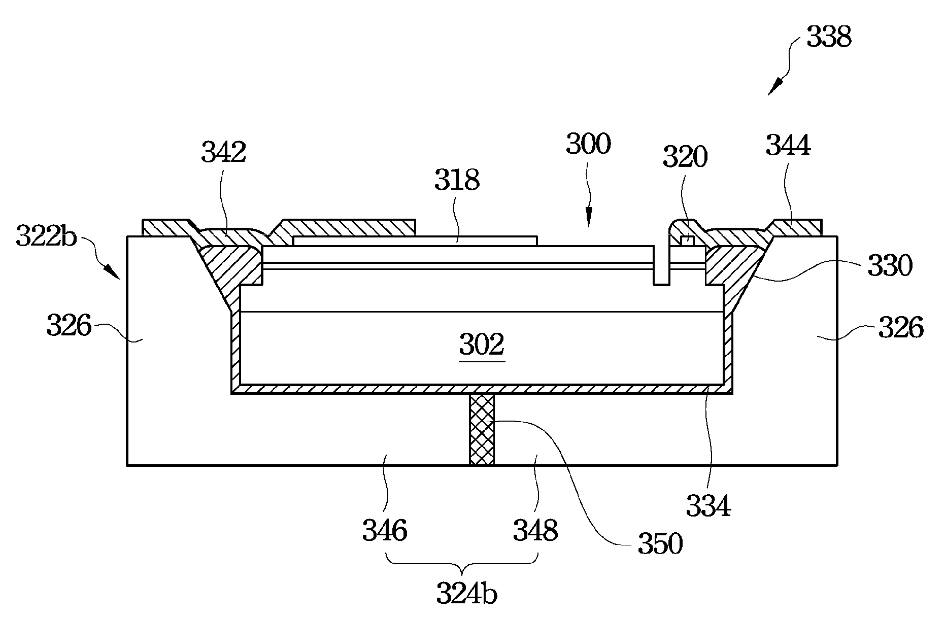
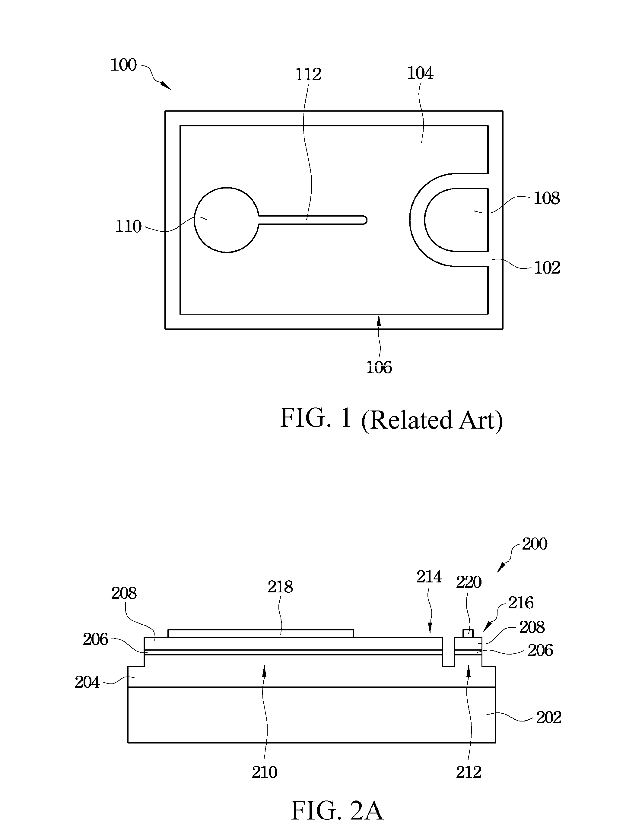
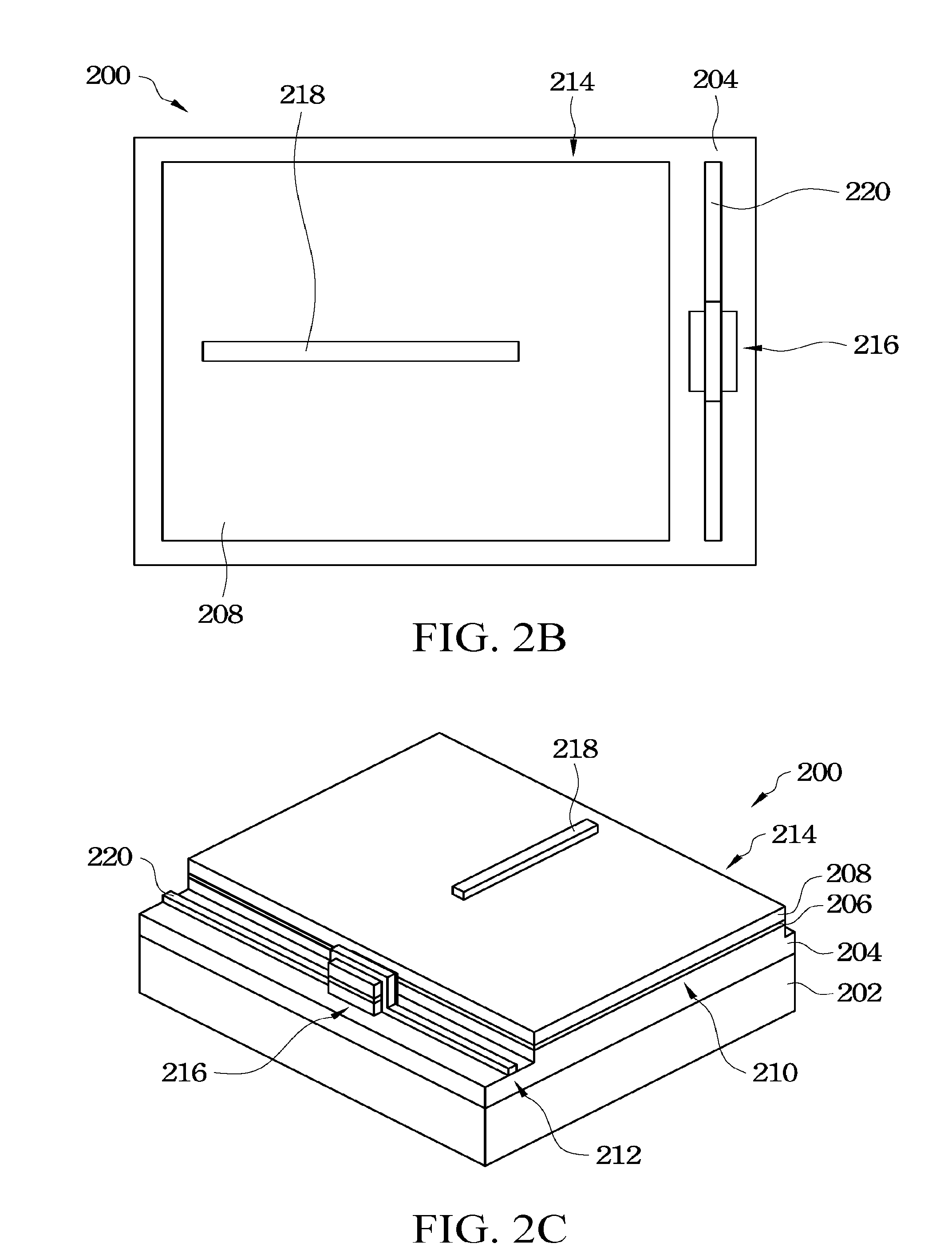
[0039]The present invention will now be described more fully hereinafter with reference to the accompanying drawings, in which exemplary embodiments of the invention are shown. This invention may, however, be embodied in many different forms and should not be construed as limited to the embodiments set forth herein. Rather, these embodiments are provided so that this disclosure will be thorough and complete, and will fully convey the scope of the invention to those skilled in the art. Like reference numerals refer to like elements throughout.

[0040]Example embodiments are described herein with reference to cross-sectional illustrations that are schematic illustrations of idealized embodiments (and intermediate structures) of example embodiments. As such, variations from the shapes of the illustrations as a result, for example, of manufacturing techniques and / or tolerances, are to be expected. Thus, example embodiments should not be construed as limited to the shapes of regions illust...


PUM


Abstract

A light-emitting diode (LED) structure and a method for manufacturing the same. In one embodiment, the LED structure includes a carrying component, an LED chip, a first conductivity type electrode and a second conductivity type electrode. The carrying component includes a carrier, a sidewall disposed on the carrier and forms a carrying tank. The LED chip is fixed within the carrying tank and includes a first conductivity type semiconductor layer having a first region and a second region, an active layer and a second conductivity type semiconductor layer stacked in sequence. The LED chip further includes a second conductive finger disposed on the second semiconductor layer in the first region, and a first conductive finger disposed on the first semiconductor layer in the second region. The first electrode extends on the sidewall and the first conductive finger. The second electrode extends on the sidewall and the second conductive finger.

Description

CROSS-REFERENCE TO RELATED PATENT APPLICATION[0001]This non-provisional application claims priority under 35 U.S.C. §119(a) on Patent Application No. 099146652 filed in Taiwan, R.O.C. on Dec. 29, 2010, the entire contents of which are hereby incorporated by reference.FIELD OF THE INVENTION[0002]The present invention relates to a light-emitting device and a method for manufacturing the same, and more particularly to a light-emitting diode (LED) structure and a method for manufacturing the same.BACKGROUND OF THE INVENTION[0003]In the techniques for manufacturing an LED device, with the development of the epitaxial technique and improvement of the chip manufacturing technique, the luminous efficiency of the LED is continuously increased. Therefore, a high luminance performance can be achieved even if the LED device is downsized.[0004]FIG. 1 is a top view of a conventional LED. In the conventional LED 100, an n-type electrode 108 is disposed on an n-type semiconductor layer 102, and a p...

Claims


Application Information

Patent Timeline
IPC IPC(8): H01L33/60
CPCH01L24/24H01L33/20H01L33/44H01L33/486H01L33/62H01L2224/24247H01L2224/32245H01L2224/73267H01L2224/92244H01L2924/12041H01L2924/15153H01L2924/00
Inventor YU, KUOHUIWANG, CHIENCHUNCHU, CHANGHSINWU, HAOCHING
Owner CHI MEI LIGHTING TECH
Why Eureka
Try Eureka