LED lamps

a led lamp and led light technology, applied in the field of colored and white led lamps, can solve the problems of reducing the use of single-chip led lamps, affecting the efficiency of led traffic lights, and requiring many led lamps to provide single led traffic lights, so as to avoid or reduce the need for clustering

Inactive Publication Date: 2012-07-05
EPISTAR CORP
View PDF2 Cites 4 Cited by
  • Summary
  • Abstract
  • Description
  • Claims
  • Application Information

AI Technical Summary

Benefits of technology

[0009]An object of the present invention is to provide a single-chip LED lamp that avoids or reduces the need for clustering.A further object of the present invention is to provide a single chip LED lamp arranged so that light emitting portions of the chip are adjusted to be equalised in intensity.
[0010]A further object of the present invention is to provide a single chip LED lamp in which the sizes of the bonding pads relative to the size of the chip are reduced, so as to improve uniformity of light projected by a lensed lamp.
[0011]A further object of the present invention is to provide a single chip LED lamp, with input power in the region of 5-25 watts, that has low rise of the junction temperature when energised, thus prolonging the life of the lamp and reducing or eliminating the need for forced ventilation of the lamp.A further object of the present invention is to provide a single chip LED lamp arranged so that light emitting portions of the chip that are faulty, by drawing more than their fair share of current, are starved of electrical power.

Problems solved by technology

Providing a lamp unit by clustering single-chip LED lamps is very costly, since it involves making several single-chip lamps, housing them in a unit, wiring them up, and testing the final unit.
The need to use many LED lamps to provide a single LED traffic light is a disadvantage, particularly since only one tungsten light source is needed for a conventional traffic light.
Prior art single-chip LED lamps having clear convergent lenses, used widely in outdoor displays, suffer not only from the fact that they are of low power but also from the fact that they project light that is not uniform.
The non-uniformity is partly due to the bonding pad or pads on the chip top face, which are projected by the lamp as dark areas.
The typical width of the bonding pad is about 30-40% of the width of the chip and this is large enough to interfere with achieving good uniformity of projected light even if the LED lens is defocussed relative to top face of the chip.

Method used


Image

  • LED lamps
  • LED lamps
  • LED lamps

Examples


Embodiment Construction

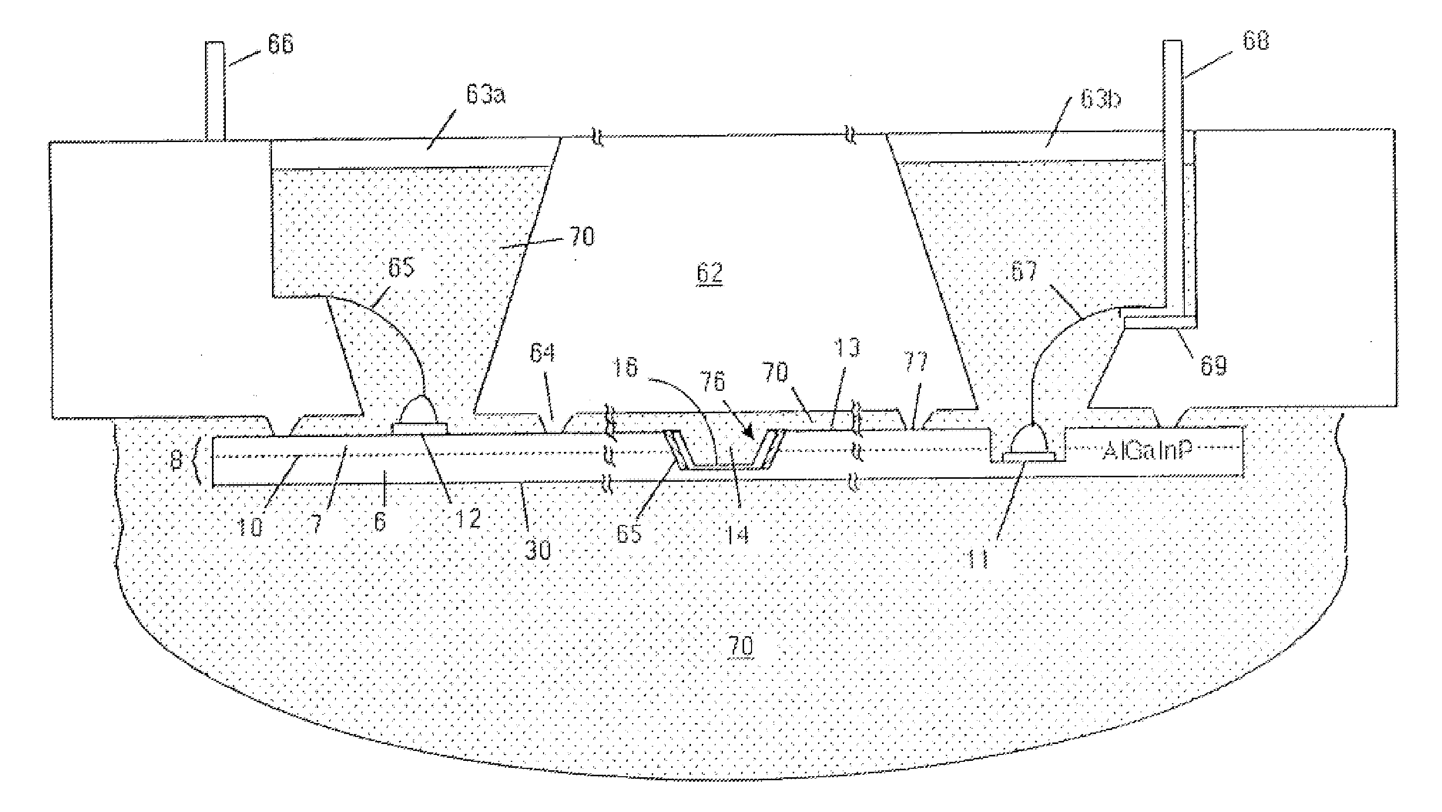
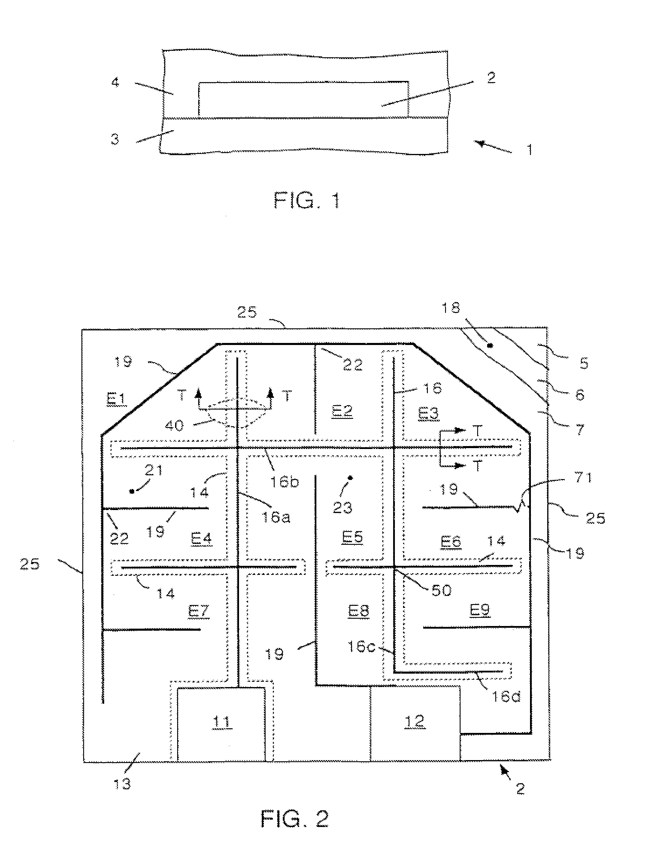
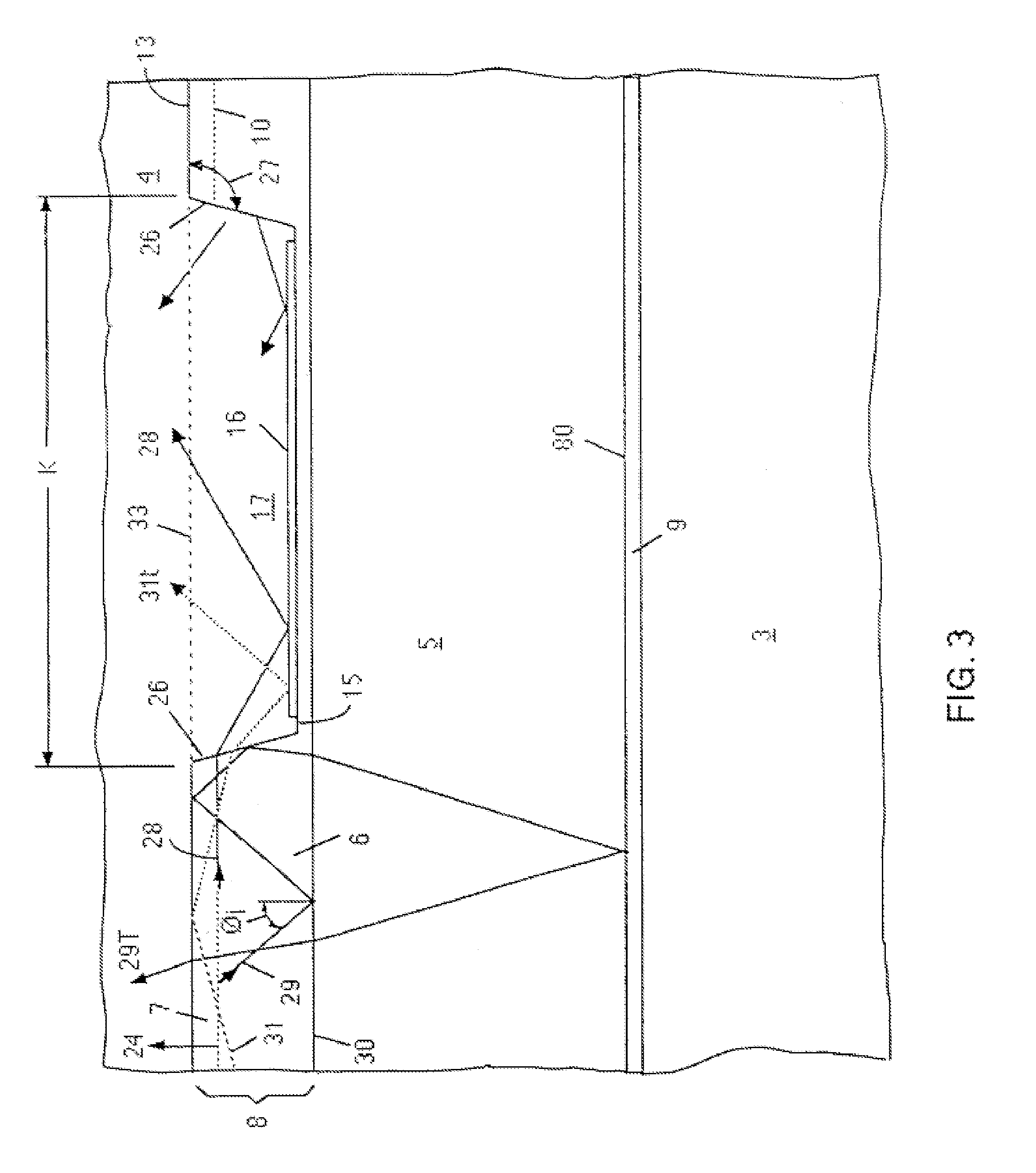
[0058]FIGS. 1-3 illustrate an improved LED light source according to an embodiment of the invention. Light source 1 comprises an LED chip 2 mounted on a metal support 3 which may be part of a reflective bowl the floor of which acts as a heat sink. Over chip 2 there is a cover 4 of transparent dielectric material. FIG. 3 is a sectional view taken along T-T of a portion 40 of chip 2.

[0059]Chip 2 comprises a transparent base 5 over which is formed a layer 6 of n-type semiconductor material. A layer 7 of p-type semiconductor material is formed over n-layer 6. Each of semiconductor layers 6, 7 can be less than 5 microns thick. Semiconductor layers 6, 7 are referred to collectively as semiconductor 8. Each of the basic n, p layers 6, 7 may include supplementary layers, not shown, that enhance the performance of the chip, or that simplify its manufacture. For example, p-layer 7 may include a thin light-passing gold layer on top of it to, in effect, enhance the electrical conductivity of th...


PUM


Abstract

A high power LED lamp has a GaN chip placed over an AlGaInP chip. A reflector is placed between the two chips. Each of the chips has trenches diverting light for output. The chip pair can be arranged to produce white light having a spectral distribution in the red to blue region that is close to that of daylight. Also, the chip pair can be used to provide an RGB lamp or a red-amber-green traffic lamp. The active regions of both chips can be less than 50 microns away from a heat sink.

Description

CROSS-REFERENCE TO RELATED APPLICATIONS[0001]This application is a continuation of U.S. patent application Ser. No. 13 / 331,871 filed on Dec. 20, 2011, which is continuation of U.S. patent application Ser. No. 13 / 064,899 filed on Apr. 25, 2011, which is a continuation of U.S. patent application Ser. No. 11 / 475,021 filed on Jun. 27, 2006, now U.S. Pat. No. 7,947,998, which was a continuation of application Ser. No. 10 / 678,174, filed Oct. 6, 2003, now abandoned, which was a continuation of application Ser. No. 09 / 820,912, filed Mar. 30, 2001, now U.S. Pat. No. 6,633,120, which was a continuation-in-part of application Ser. No. 09 / 549,575 filed Apr. 14, 2000, now abandoned, which was a continuation-in-part of application Ser. No. 09 / 196,358, filed Nov. 19, 1998, now U.S. Pat. No. 6,346,771, which claims foreign priority to application Serial No. 9724507.0 filed in the United Kingdom on Nov. 19, 1997, which claims foreign priority to application Serial No. 9820311.0 filed in the United K...

Claims


Application Information

Patent Timeline
Patent Type & Authority Applications(United States)
IPC IPC(8): H01L33/44H01L33/00H01L33/20H01L33/38
CPCF21K9/00H01L33/0079H01L33/46H01L33/38H01L33/20H01L2224/4824H01L2224/48465H01L33/0093H01L2924/00
Inventor HASSAN, SALAM P. A.
Owner EPISTAR CORP
Why Eureka
Try Eureka