High Power Semiconductor Package with Conductive Clip and Flip Chip Driver IC with Integrated Control Transistor
What is Al technical title?
Al technical title is built by PatSnap Al team. It summarizes the technical point description of the patent document.
a high-power, semiconductor technology, applied in semiconductor devices, semiconductor/solid-state device details, electrical apparatus, etc., can solve problems such as inability to meet the requirements of the package, increase the electrical resistance, and reduce the current carrying capacity
Active Publication Date: 2012-07-05
INFINEON TECH AMERICAS CORP
View PDF21 Cites 25 Cited by
Summary
Abstract
Description
Claims
Application Information
AI Technical Summary
This helps you quickly interpret patents by identifying the three key elements:
Problems solved by technology
Method used
Benefits of technology
[0009]A high power semiconductor package with conductive clip and flip chip driver IC with integrated control transistor, substantially as shown in and / or described in connection with at least one of the figures, and as set forth more completely in the claims.
Problems solved by technology
Unfortunately, conventional high power semiconductor package designs use wirebonds for transistor interconnections, undesirably increasing electrical resistance while reducing current carrying capacity.
Additionally, by following conventional package design rules to successfully accommodate such wirebonds, package form factor and complexity may undesirably increase.
For example, package height may be increased to provide sufficient wirebond loop height, lateral package size may be increased to avoid wire crossing and the potential for wire shorting, and additional area on the package may be reserved for bond pad connections, thereby undesirably reducing package power density.
Additionally, the increased package complexity resulting from the wirebonds may negatively affect manufacturing time, cost, and package yields.
Method used
Image
Click on the blue label to locate the original text in one second.
Reading with bidirectional positioning of images and text.
Examples
Embodiment Construction
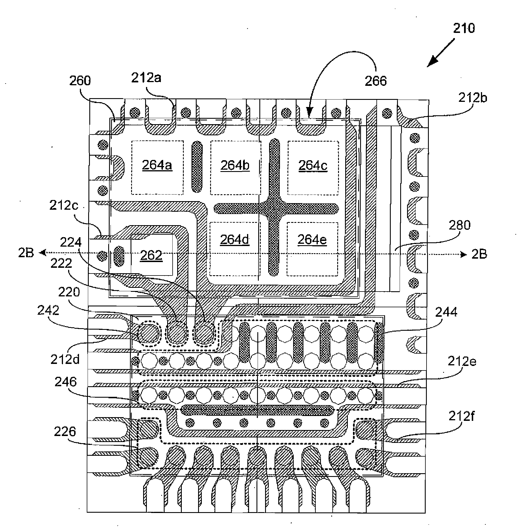
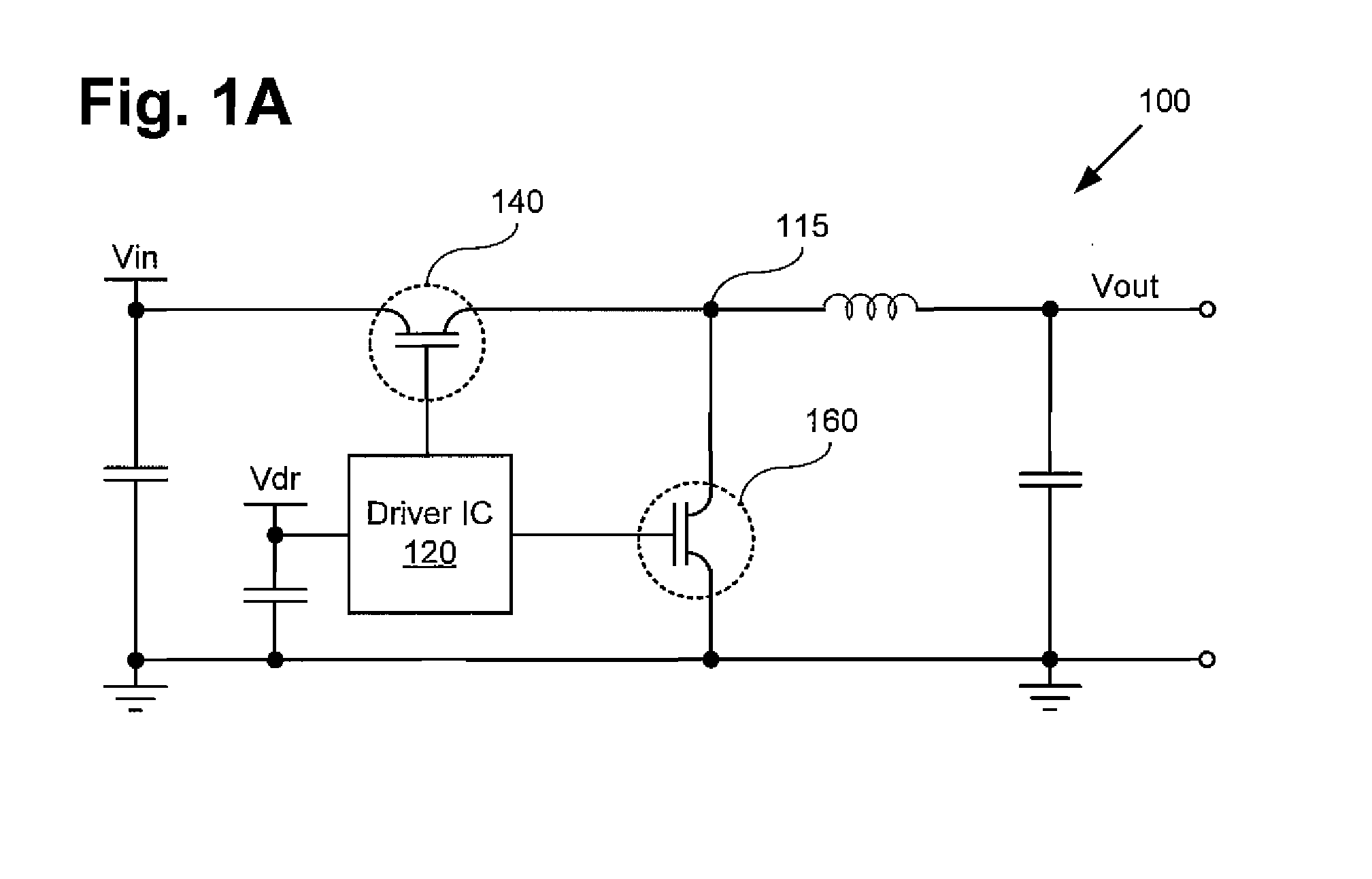
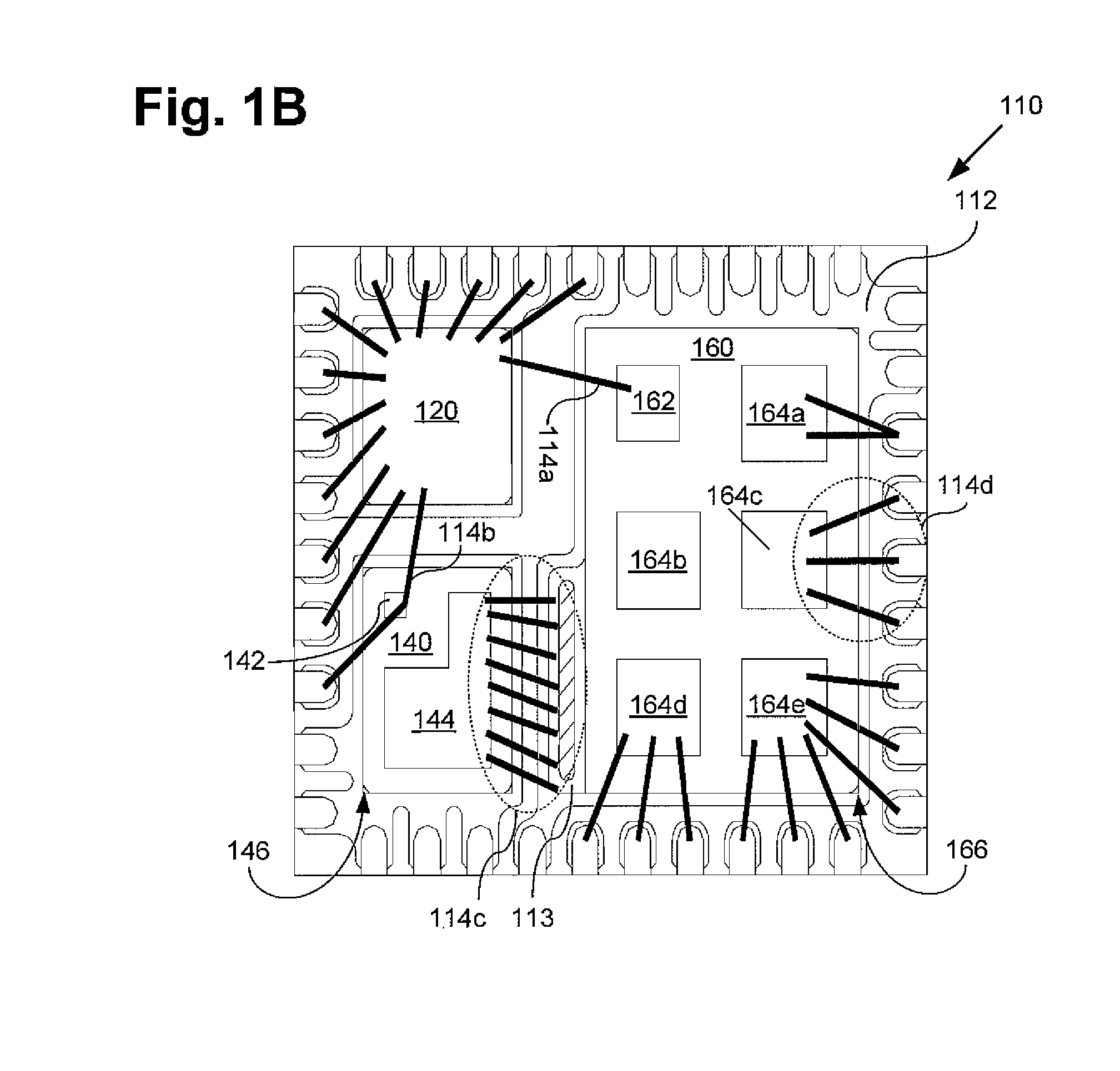
[0014]The present application is directed to a high power semiconductor package with conductive clip and a flip chip driver IC with integrated control transistor. The following description contains specific information pertaining to the implementation of the present invention. One skilled in the art will recognize that the present invention may be implemented in a manner different from that specifically discussed in the present application. Moreover, some of the specific details of the invention are not discussed in order not to obscure the invention. The specific details not described in the present application are within the knowledge of a person of ordinary skill in the art.
[0015]The drawings in the present application and their accompanying detailed description are directed to merely exemplary embodiments of the invention. To maintain brevity, other embodiments of the invention, which use the principles of the present invention, are not specifically described in the present appl...
PUM
Abstract
One exemplary disclosed embodiment comprises a high power semiconductor package configured as a buck converter having a sync transistor with a top surface having a drain, a flip chip driver integrated circuit (IC) having an integrated control transistor, the flip chip driver IC driving the sync and control transistors, and a conductive clip electrically coupling the drain of the sync transistor to a common portion of the leadframe shared with a control source of the control transistor. In this manner, the leadframe and the conductive clip provide efficient current conduction by direct mechanical connection and large surface area conduction, significantly reducing package electrical resistance, form factor, complexity, and cost compared to conventional packages. Moreover, by integrating only the control transistor rather than both the control and sync transistor within the flip chip driver IC, the sync transistor may remain separate, simplifying manufacture and providing greater total surface area for thermal dissipation.
Description
BACKGROUND OF THE INVENTION[0001]The present application claims the benefit of and priority to a pending provisional application entitled “Metal Clip for Efficient, Low Cost Package with Improved Current Carrying Capability and Reduced Form Factor and with Application in Buck Converters,” Ser. No. 61 / 460,553 filed on Jan. 3, 2011. The disclosure in that pending provisional application is hereby incorporated fully by reference into the present application. Additionally, pending applications Ser. No. 11 / 986,848, filed on Nov. 27, 2007, titled “Synchronous DC / DC Converter,” and Ser. No. 12 / 928,102, filed on Dec. 3, 2010, titled “DC / DC Converter with Depletion-Mode III-Nitride Switches,” are also incorporated fully by reference into the present application.DEFINITION[0002]In the present application, “III-nitride” (or “III-Nitride”) refers to a compound semiconductor that includes nitrogen and at least one group III element, such as, but not limited to, GaN, AlGaN, InN, AlN, InGaN, InAlG...
Claims
Application Information
Patent Timeline
Application Date:The date an application was filed.
Publication Date:The date a patent or application was officially published.
First Publication Date:The earliest publication date of a patent with the same application number.
Issue Date:Publication date of the patent grant document.
PCT Entry Date:The Entry date of PCT National Phase.
Estimated Expiry Date:The statutory expiry date of a patent right according to the Patent Law, and it is the longest term of protection that the patent right can achieve without the termination of the patent right due to other reasons(Term extension factor has been taken into account ).
Invalid Date:Actual expiry date is based on effective date or publication date of legal transaction data of invalid patent.
Patent Type & Authority Applications(United States)