Organic Light Emitting Diode Display and Manufacturing Method of the Same

Active Publication Date: 2012-07-05
SAMSUNG DISPLAY CO LTD
View PDF6 Cites 41 Cited by
  • Summary
  • Abstract
  • Description
  • Claims
  • Application Information

AI Technical Summary

Benefits of technology

[0035]According to exemplary embodiments, the sealing member is formed to be at least partially overlapped with the circuit unit at the outer side of the display substrate so that the dead space can be reduced.
[0036]Further, the s

Problems solved by technology

A circuit unit or a wire unit that electrically connects the organic light emitting element with external devices is formed on the display substrate of the OLED display,

Method used


Image

  • Organic Light Emitting Diode Display and Manufacturing Method of the Same
  • Organic Light Emitting Diode Display and Manufacturing Method of the Same
  • Organic Light Emitting Diode Display and Manufacturing Method of the Same

Examples


Embodiment Construction

[0040]The present invention will be described more fully hereinafter with reference to the accompanying drawings, in which exemplary embodiments of the invention are shown.

[0041]The drawings and description are to be regarded as illustrative in nature and not restrictive. Like reference numerals designate like elements throughout the specification. In the drawings, for better understanding and ease of description, thicknesses of some layers and areas are excessively displayed, but the present invention is not limited thereto.

[0042]It will be understood that when an element such as a layer, film, region, or substrate is referred to as being “on” another element, it can be directly on the other element or intervening elements may also be present therebetween.

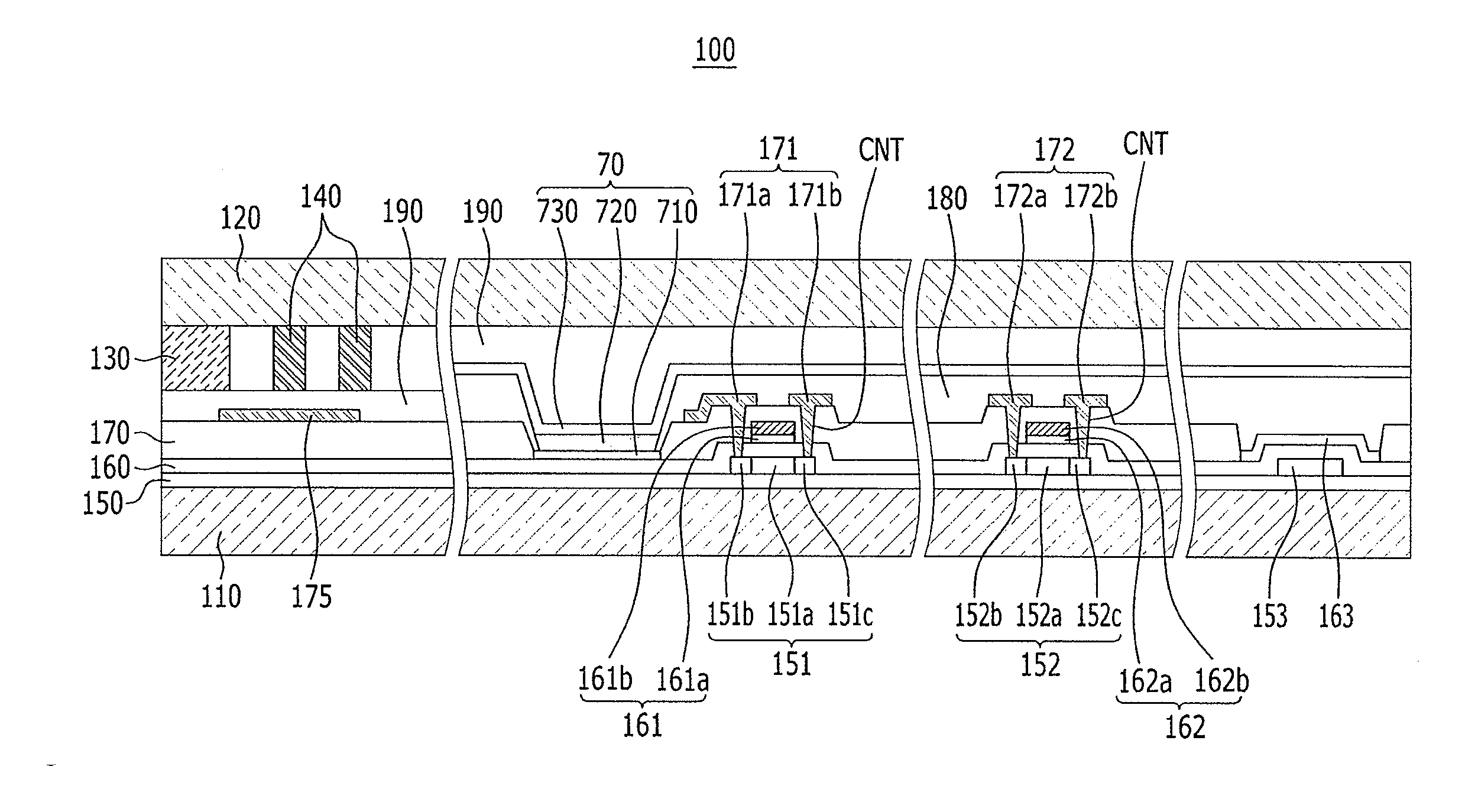
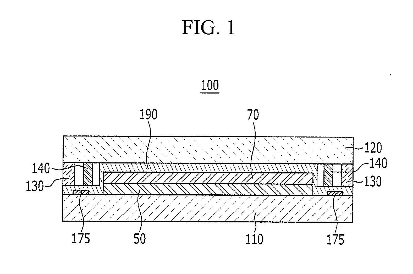
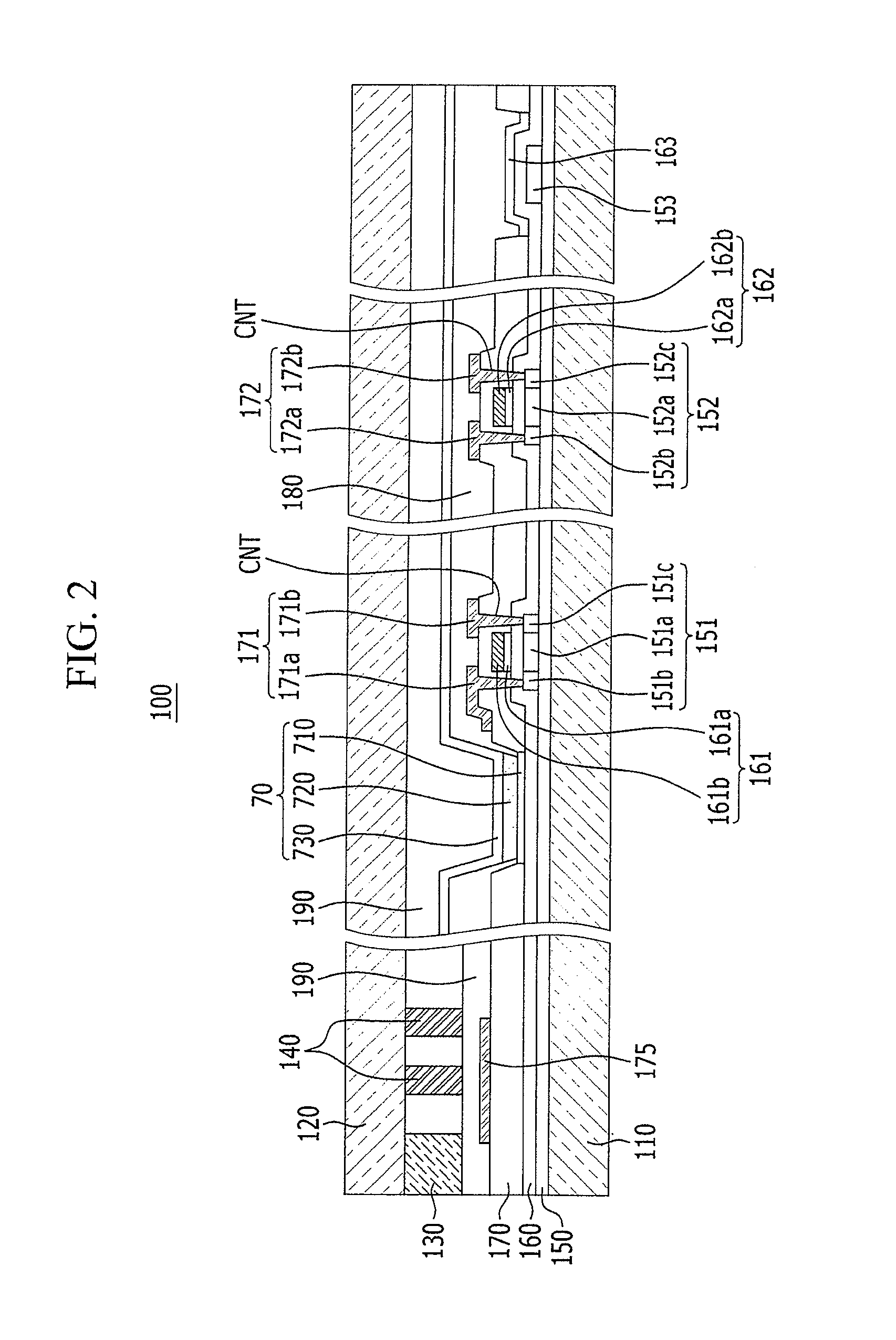
[0043]FIG. 1 is a schematic cross-sectional view of an organic light emitting diode (OLED) display according to an exemplary embodiment, and a configuration of an OLED display 100 according to the present exemplary embodiment will...


PUM


Abstract

An organic light emitting diode (OLED) display includes: a first substrate including a display area and a non-display area; a driving element on the display area of the first substrate, and including a driving thin film transistor, a switching thin film transistor, and a capacitor; a circuit unit on the non-display area of the first substrate; an organic light emitting element on the driving element, and including a pixel electrode, an organic emission layer, and a common electrode; an inorganic protective layer covering the circuit unit and the common electrode of the organic light emitting diode; a sealing member on the inorganic protective layer in the non-display area of the first substrate; and a second substrate on the sealing member.

Description

CROSS-REFERENCE TO RELATED APPLICATIONS[0001]This application claims priority to and the benefit of Korean Patent Application No. 10-2010-0139428, filed in the Korean Intellectual Property Office, on Dec. 30, 2010, the entire content of which is incorporated herein by reference.BACKGROUND[0002]1. Field[0003]The described technology relates generally to an organic light emitting diode (OLED) display and a manufacturing method thereof.[0004]2. Description of Related Art[0005]An organic light emitting diode (OLED) display is a flat panel display which can be made lightweight and thin because it has a self-luminous characteristic and requires no separate light source. Particularly, the OLED display exhibits quality characteristics such as low power consumption, high luminance, high response speed, and as such, the OLED display receives much attention as a next-generation display device.[0006]In general, an OLED display includes an organic light emitting element and a thin film transisto...

Claims


Application Information

Patent Timeline
IPC IPC(8): H01L27/32H01J9/26
CPCH01L27/3244H01L51/5246H01L51/56H01L51/5259H01L51/5253H10K59/12H10K50/8426H10K50/844H10K50/846H10K71/00
Inventor YOU, CHUN-GICHOI, JOON-HOO
Owner SAMSUNG DISPLAY CO LTD
Why Eureka
Try Eureka