Solid-state image pickup device

a solid-state image and pickup device technology, applied in the direction of color television details, television system details, television systems, etc., can solve the problems of a/d conversion error a/d conversion error, etc., to achieve the effect of minimal suppression of the increase in the size of the solid-state image pickup device, high degree of accuracy and high degree of accuracy

Active Publication Date: 2012-07-12
OLYMPUS CORP
View PDF6 Cites 19 Cited by
  • Summary
  • Abstract
  • Description
  • Claims
  • Application Information

AI Technical Summary

Benefits of technology

[0036]According to the present invention, by comparing the output signal of the first upper bit latch unit with the output signal of the second upper bit latch unit and correcting the count value based on the comparison result and the output signal of the lower bit latch unit, it is possible to obtain the count value when the lower bit latch unit latches the output signals of the plurality of delay elements, and thus A / D conversion can be performed with a high degree of accuracy. Further, since the number of bits of the first upper bit latch unit 105 can be reduced to be smaller than the number of bits of the counter unit, an increase in the size of the solid state image pickup device can be minimally-suppressed.
[0037]According to the present invention, by comparing the output signal of the first counter / latch unit, the output signal of the second counter / latch unit, and the output signal of the third counter / latch unit and correcting the count value based on the comparison result and the output signal of the lower bit latch unit, it is possible to obtain the count value when the lower bit latch unit latches the output signals of the plurality of delay elements, and thus A / D conversion can be performed with a high degree of accuracy. Further, since the number of bits of the second counter / latch unit and the number of bits of the third counter / latch unit can be reduced to be smaller than the number of bits of the first counter / latch unit, an increase in the size of the solid state image pickup device can be minimally-suppressed.
[0038]According to the present invention, by comparing the output signal of the first counter / latch unit with the output signal of the second counter / latch unit and correcting the count value based on the comparison result and the output signal of the lower bit latch unit, it is possible to obtain the count value when the lower bit latch unit latches the output signals of the plurality of delay elements, and thus A / D conversion can be performed with a high degree of accuracy. Further, since the number of bits of the second counter / latch unit can be reduced to be smaller than the number of bits of the first counter / latch unit, an increase in the size of the solid state image pickup device can be minimally-suppressed.

Problems solved by technology

However, when the above described A / D converter is employed in a CMOS image sensor (a CMOS image sensor of a column analog-to-digital converter (ADC) type) which is an example of a CMOS image sensor and includes an A / D converter arranged for each pixel column or for a plurality of pixel columns, the following problems occur.
Due to the delay, a timing at which the control signal 010 reaches the pulse delay unit / latch unit 0051 is different from a timing at which the control signal 010 reaches the counter unit 0052 (specifically, a timing at which the control signal 010 reaches the counter unit 0052 is delayed), so that an error may occur in the A / D conversion result.
However, depending on the line layout of the control signal 010, the delay of the control signal 010 may occur in the pulse delay unit / latch unit 0051, and the counter unit 0052 may perform erroneous count (minus one different), leading to an error in the A / D conversion result.
However, when the delay of the control signal 010 occurs in the counter unit 0052, the error occurs in the A / D conversion result as described above.
Further, even when there is no difference (or a small difference) in the line length of the signal line, a random signal deviation may occur due to overlapping of a clock signal from another signal line.

Method used


Image

  • Solid-state image pickup device
  • Solid-state image pickup device
  • Solid-state image pickup device

Examples


first preferred embodiment

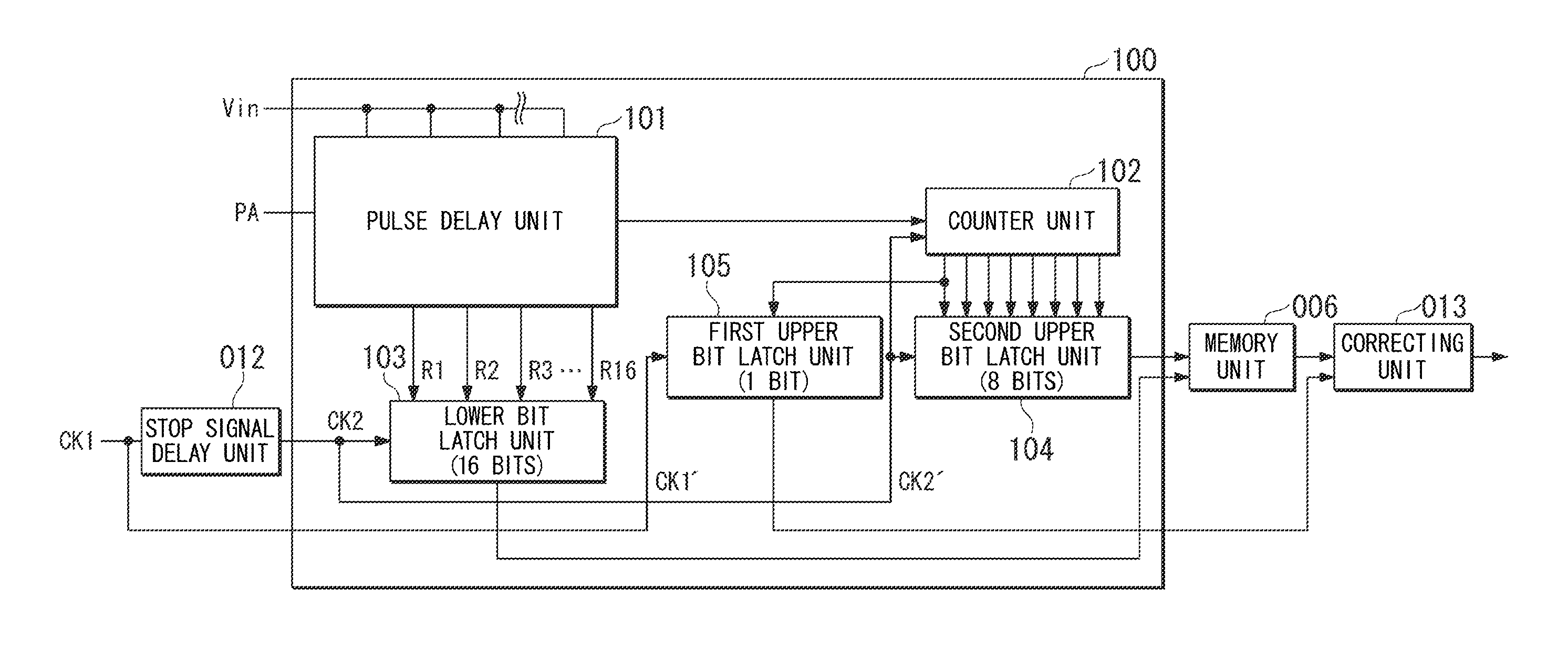
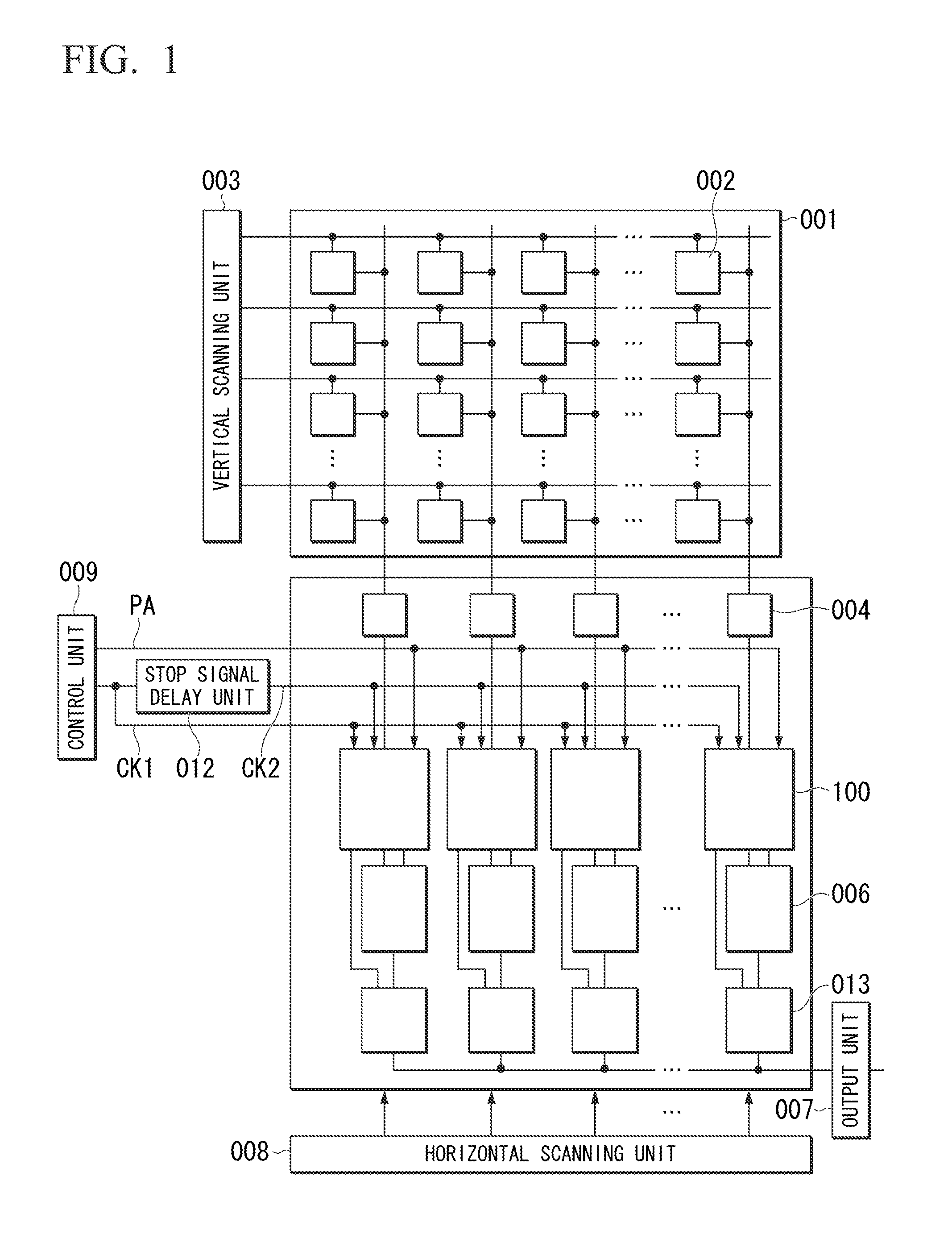
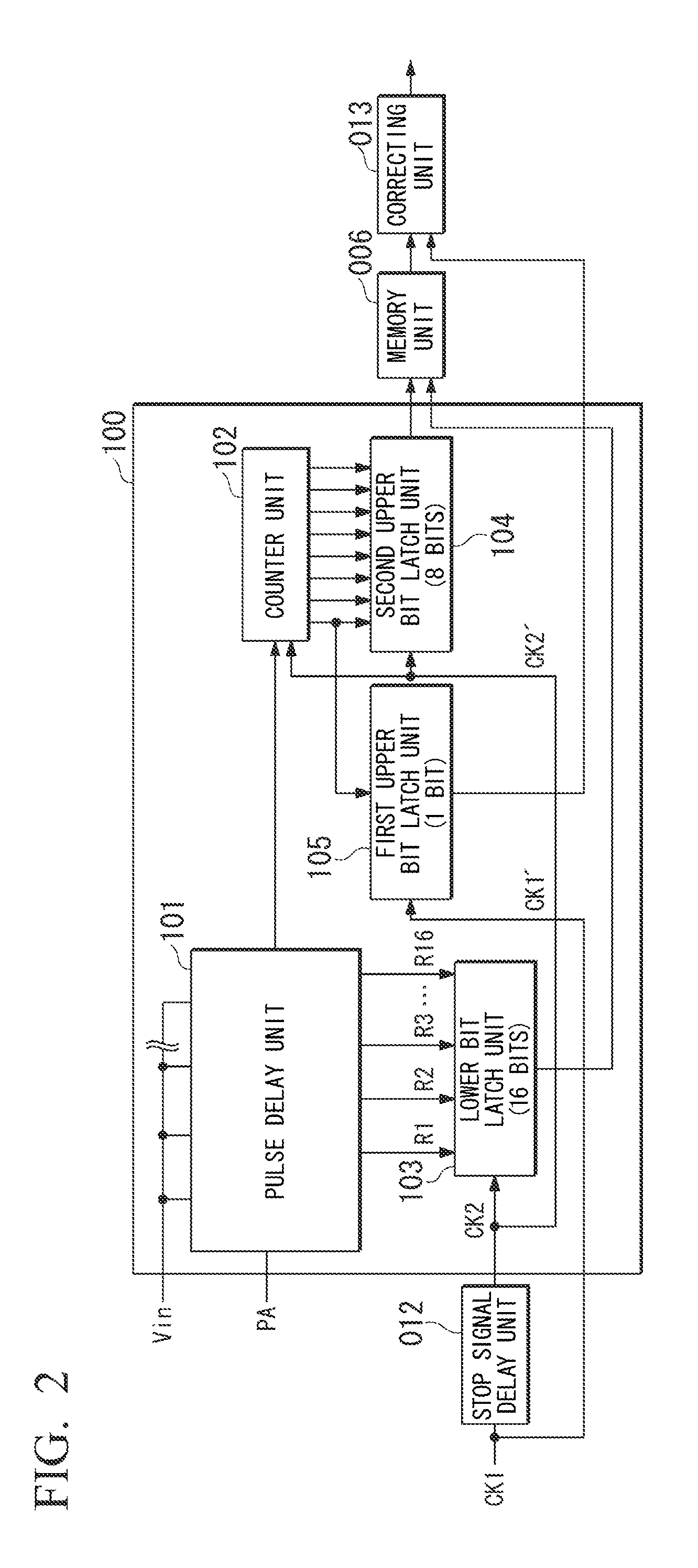
[0065]A first preferred embodiment of the present invention will be described. FIG. 1 is a block diagram illustrating a configuration of a solid state image pickup device in accordance with the first preferred embodiment of the present invention. FIG. 2 is a block diagram illustrating a configuration of an A / D converter arranged in the solid state image pickup device in accordance with the first preferred embodiment of the present invention. Components in the drawings will be described below. For convenience of description, preferred embodiments of the present invention will be described in connection with a detailed configuration of a solid state image pickup device, and a detailed configuration and operation of an A / D converter. That is, a detailed operation of a solid state image pickup device is the same as an operation of a solid state image pickup device of the related art or the above described operation, and thus a description thereof will be omitted here.

[0066]In addition, ...

second preferred embodiment

[0107]A second preferred embodiment of the present invention will be described. FIG. 8 is a block diagram illustrating a configuration of a solid state image pickup device in accordance with the second preferred embodiment of the present invention. FIG. 9 is a block diagram illustrating a configuration of an A / D converter 200 arranged in the solid state image pickup device in accordance with the second preferred embodiment of the present invention. Among components illustrated in FIGS. 8 and 9, the same components as in FIGS. 1 and 2 are denoted by the same reference numerals, and thus a redundant description will not be repeated here. Further, each configuration and operation in accordance with the second preferred embodiment of the present invention will be described below focusing on the differences with the first preferred embodiment.

[0108]The difference between the first preferred embodiment and the second preferred embodiment of the present invention lies in that the A / D conve...

third preferred embodiment

[0113]A third preferred embodiment of the present invention will be described. FIG. 11 is a block diagram illustrating a configuration of a solid state image pickup device in accordance with the third preferred embodiment of the present invention. FIG. 12 is a block diagram illustrating a configuration of an A / D converter 300 arranged in the solid state image pickup device in accordance with the third preferred embodiment of the present invention. Among components illustrated in FIGS. 11 and 12, the same components as in the solid state image pickup device and the A / D converter described above are denoted by the same reference numerals, and thus a redundant description thereof will not be repeated here. Further, each configuration and operation in accordance with the third preferred embodiment of the present invention will be described below focusing on differences thereof with the first preferred embodiment.

[0114]The difference between the first preferred embodiment and the third p...


PUM


Abstract

A solid state image pickup device may include a pixel unit that includes a plurality of pixels; a pulse delay unit that includes a plurality of delay elements, each of the plurality of delay elements including a power supply terminal; a stop control unit; a stop signal delay unit; a lower bit latch unit; a counter unit; a first upper bit latch unit; a second upper bit latch unit; and a correcting unit that compares an output signal of the first upper bit latch unit with an output signal of the second upper bit latch unit, and corrects a count value, which is a count result of the counter unit, based on a comparison result and an output signal of the lower bit latch unit.

Description

BACKGROUND OF THE INVENTION[0001]1. Field of the Invention[0002]The present invention relates to a solid state image pickup device that performs analog-to-digital (A / D) conversion converting an analog voltage signal output from a pixel into binary digital data.[0003]Priority is claimed on Japanese Patent Application No. 2011-003983, filed Jan. 12, 2011, the content of which is incorporated herein by reference.[0004]2. Description of the Related Art[0005]All patents, patent applications, patent publications, scientific articles, and the like, which will hereinafter be cited or identified in the present application, will hereby be incorporated by reference in their entirety in order to describe more fully the state of the art to which the present invention pertains.[0006]In recent years, image pickup devices, such as digital cameras and digital video cameras, that acquire an imaged image as digital data using a solid state image pickup device (hereinafter referred to as an “image sens...

Claims


Application Information

Patent Timeline
Patent Type & Authority Applications(United States)
IPC IPC(8): H04N5/217
CPCH03M1/123H03M1/14H03M1/60H04N5/357H04N5/378H03M1/502H04N25/60H04N25/75
Inventor YAMAZAKI, SUSUMUHAGIHARA, YOSHIO
Owner OLYMPUS CORP
Why Eureka
Try Eureka