Method And System For A Photonic Interposer

a photonic interposer and photonic technology, applied in the field of semiconductor processing, can solve the problems of cable bulk penalties, large power requirements, and complex structure, and achieve only modest improvements in reach and limited scalability

Active Publication Date: 2012-07-12
CISCO TECH INC
View PDF8 Cites 85 Cited by
  • Summary
  • Abstract
  • Description
  • Claims
  • Application Information

AI Technical Summary

Benefits of technology

[0007]A system and/or method for a photonic interposer, substantially as shown in and/or descri

Problems solved by technology

They can be mitigated to some extent with equalization, coding, and shielding, but these techniques require considerable

Method used


Image

  • Method And System For A Photonic Interposer
  • Method And System For A Photonic Interposer
  • Method And System For A Photonic Interposer

Examples


Embodiment Construction

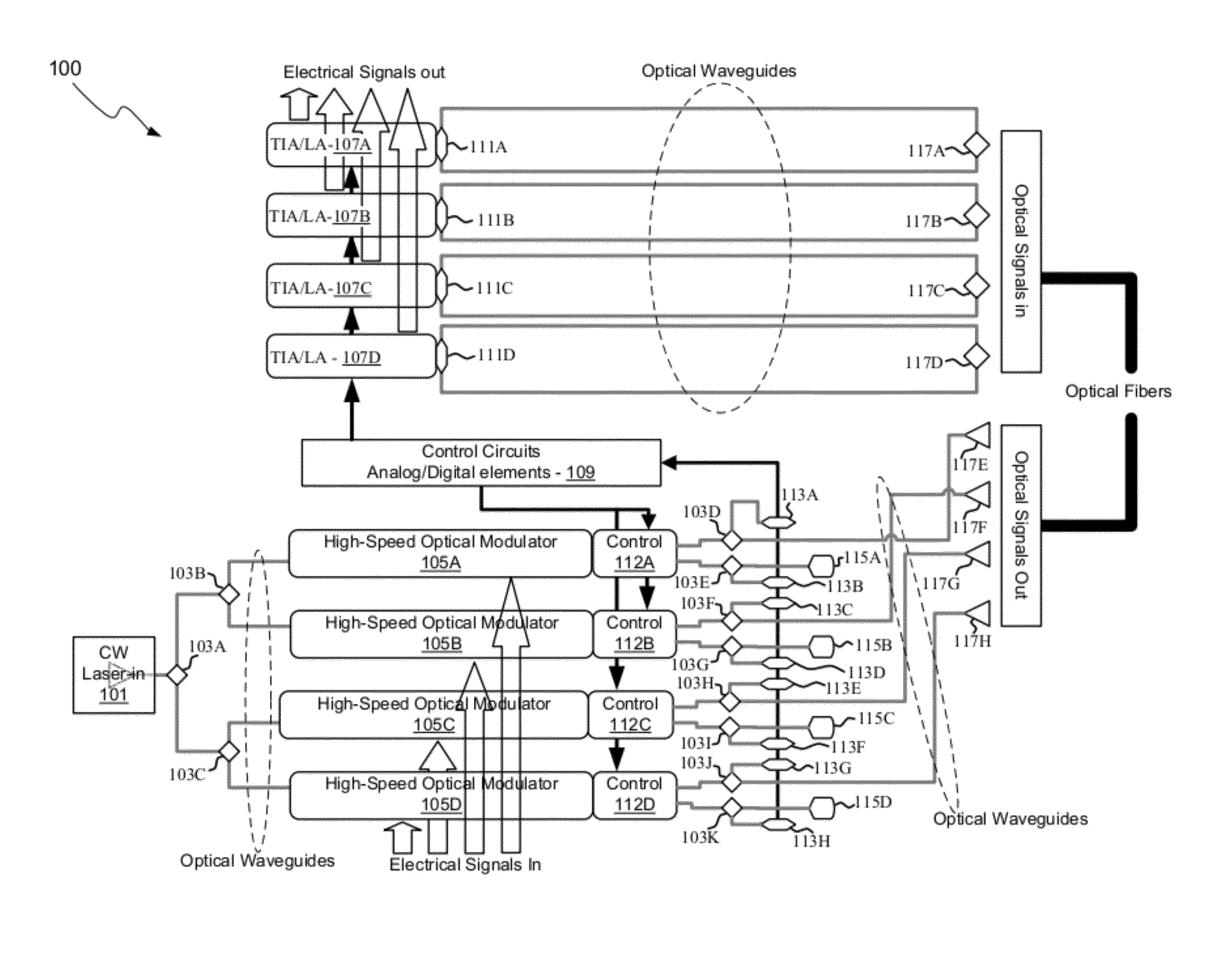
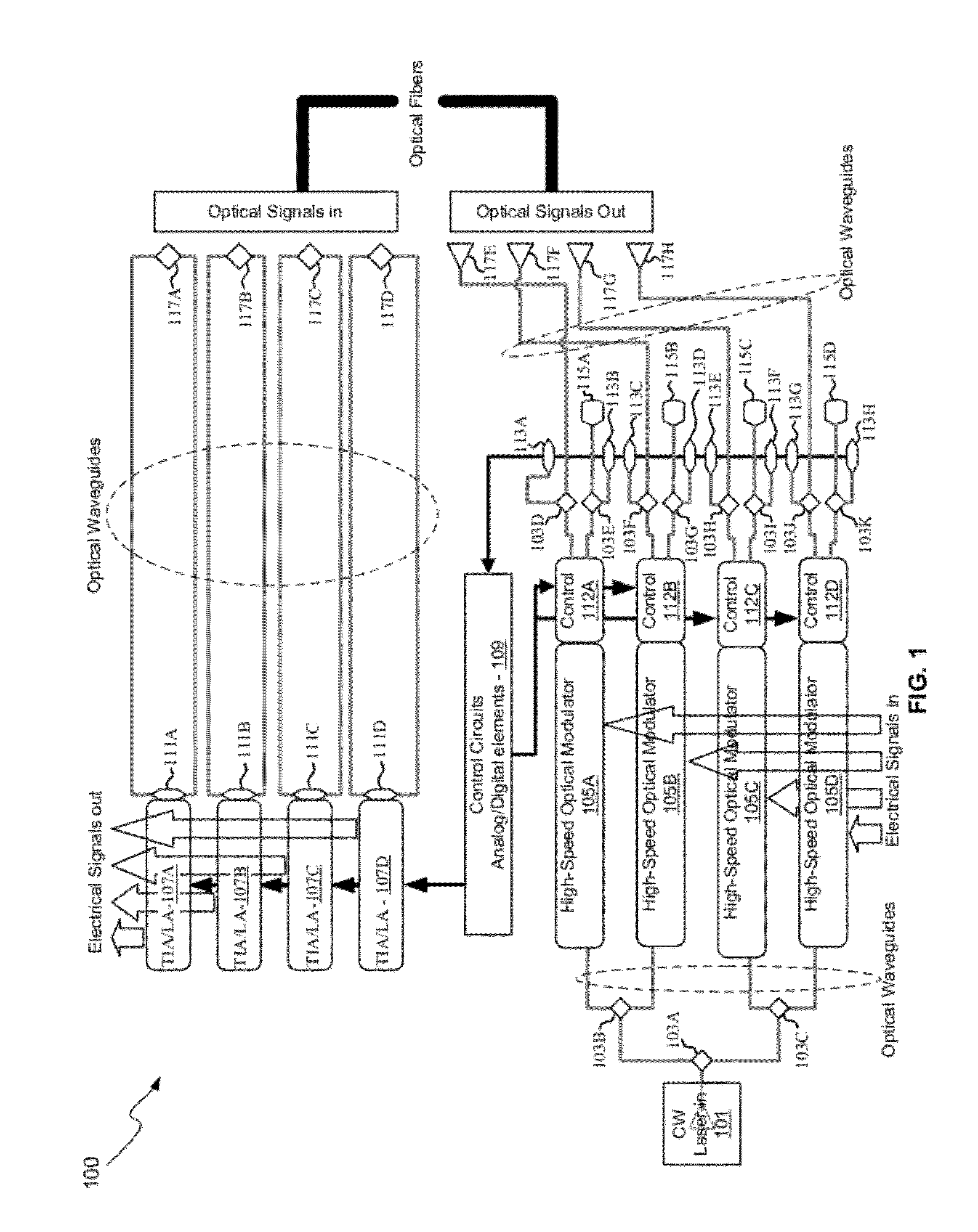
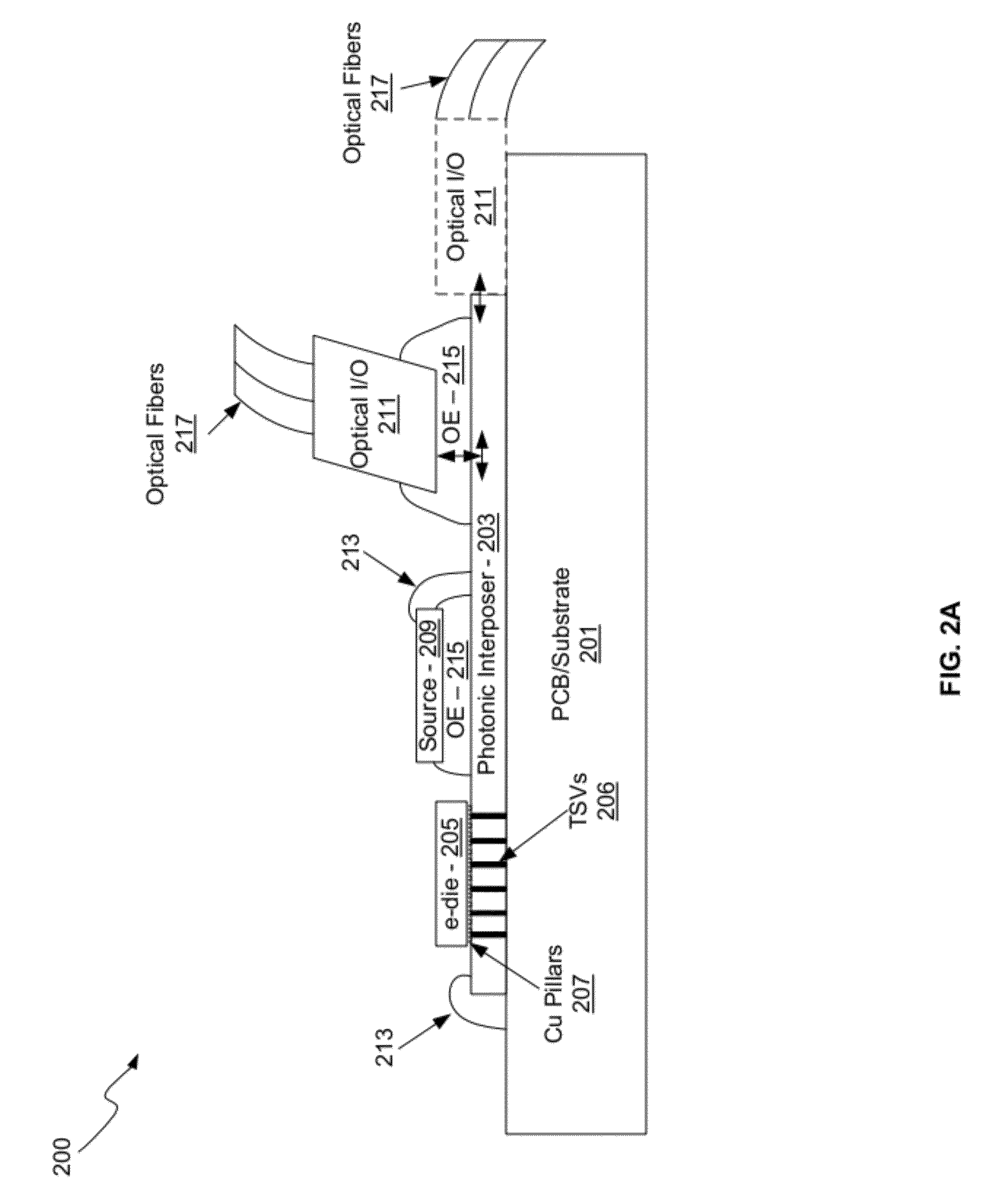
[0021]Certain aspects of the invention may be found in a method and system for a photonic interposer. Exemplary aspects of the invention may comprise receiving one or more continuous wave (CW) optical signals in a silicon photonic interposer from an optical source external to the silicon photonic interposer. The received CW optical signals may be processed based on electrical signals received from the one or more CMOS electronics die. The modulated optical signals may be received in the silicon photonic interposer from one or more optical fibers coupled to the silicon photonic interposer. Electrical signals may be generated in the silicon photonic interposer based on the received modulated optical signals. The generated electrical signals may be communicated to the one or more CMOS electronics die, via copper pillars for example. The one or more CW optical signals may be received in the silicon photonic interposer from an optical source assembly coupled to the silicon photonic inter...


PUM


Abstract

Methods and systems for a photonic interposer are disclosed and may include receiving one or more continuous wave (CW) optical signals in a silicon photonic interposer from an external optical source, either from an optical source assembly or from optical fibers coupled to the silicon photonic interposer. The received CW optical signals may be processed based on electrical signals received from the electronics die. The modulated optical signals may be received in the silicon photonic interposer from optical fibers coupled to the silicon photonic interposer. Electrical signals may be generated in the silicon photonic interposer based on the received modulated optical signals, and may then be communicated to the electronics die via copper pillars. Optical signals may be communicated into and/or out of the silicon photonic interposer utilizing grating couplers. The electronics die may comprise one or more of: a processor core, a switch core, or router.

Description

CROSS-REFERENCE TO RELATED APPLICATIONS / INCORPORATION BY REFERENCE[0001]This application is a continuation-in-part of U.S. application Ser. No. 12 / 554,449 filed on Sep. 4, 2009, and also claims priority to United States Provisional Application 61 / 516,226, filed on Mar. 30, 2011, each of which is hereby incorporated herein by reference in its entirety.FEDERALLY SPONSORED RESEARCH OR DEVELOPMENT[0002][Not Applicable]MICROFICHE / COPYRIGHT REFERENCE [0003][Not Applicable]FIELD OF THE INVENTION[0004]Certain embodiments of the invention relate to semiconductor processing. More specifically, certain embodiments of the invention relate to a method and system for a photonic interposer.BACKGROUND OF THE INVENTION[0005]As data networks scale to meet ever-increasing bandwidth requirements, the shortcomings of copper data channels are becoming apparent. Signal attenuation and crosstalk due to radiated electromagnetic energy are the main impediments encountered by designers of such systems. They c...

Claims


Application Information

Patent Timeline
IPC IPC(8): H04B10/06H04B10/02
CPCH01L21/84H01L27/1203H04B10/801H04B10/70H04B10/43H01L2224/48091H01L2224/73265H01L2924/00014G02B6/1225G02B2006/12061G02B2006/12142H01L23/49827H01L23/49838H01L23/49866H01L25/167H05K999/99
Inventor DOBBELAERE, PETER DEYOUNG, GREGPETERSON, MARK
Owner CISCO TECH INC
Why Eureka
Try Eureka