Light-emitting device package and method of manufacturing the same

a technology of light-emitting devices and manufacturing methods, which is applied in the direction of semiconductor/solid-state device manufacturing, semiconductor devices, electrical devices, etc., can solve the problems of optical quality deviation, insufficient use of light emitted through the side of the light-emitting device chip, and the density of the phosphor, so as to improve optical efficiency and manufacturing methods, and reduce optical quality deviation

Active Publication Date: 2012-07-19
SAMSUNG ELECTRONICS CO LTD
View PDF1 Cites 32 Cited by
  • Summary
  • Abstract
  • Description
  • Claims
  • Application Information

AI Technical Summary

Benefits of technology

[0008]Provided are light-emitting device packages having reduced optical quality deviation and improved optical efficiency and methods of manufacturing the same.

Problems solved by technology

However, in the light-emitting device package manufactured as above, the density of the phosphor is not uniform and thus optical quality deviation may be generated.
Also, light emitted through the side of the light-emitting device chip may not be sufficiently used.

Method used


Image

  • Light-emitting device package and method of manufacturing the same
  • Light-emitting device package and method of manufacturing the same
  • Light-emitting device package and method of manufacturing the same

Examples


Embodiment Construction

[0040]Hereinafter, a method and apparatus for manufacturing a white light-emitting device according to one or more embodiment of the present invention will be described in detail with reference to the accompanying drawings. In the drawings, like reference numerals denote like elements and sizes of each element are exaggerated for clarity.

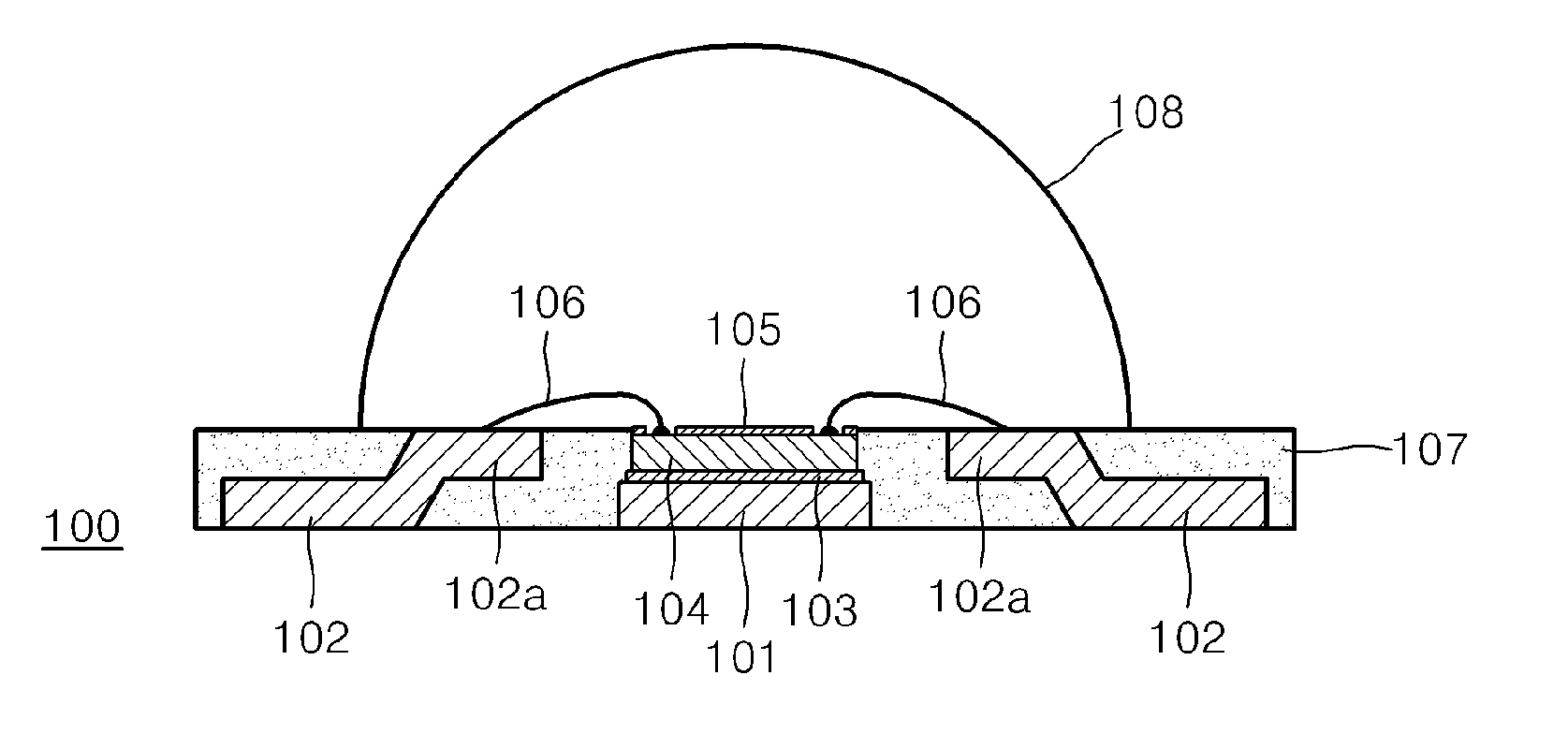
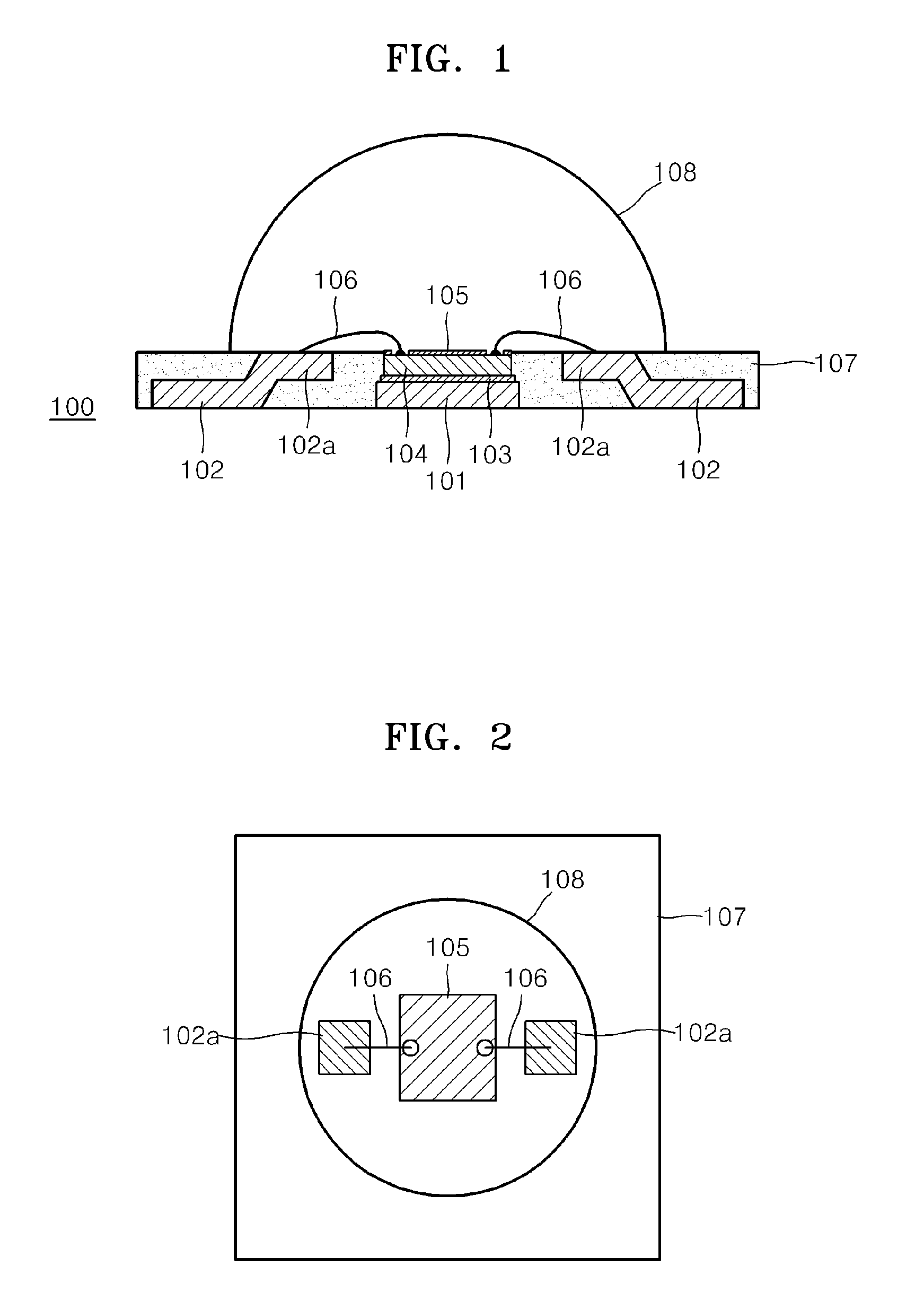
[0041]FIG. 1 is a cross-sectional view schematically illustrating a light-emitting device package 100 according to an embodiment of the present invention. Referring to FIG. 1, the light-emitting device package 100 may include a heat dissipation pad 101, a light-emitting device 104 disposed on the heat dissipation pad 101, a pair of lead frames 102 spaced apart from the heat dissipation pad 101 at both sides of the heat dissipation pad 101, a molding member 107 formed to surround the heat dissipation pad 101 and the lead frames 103, and a pair of bonding wires 106 electrically connecting the lead frames 102 and the light-emitting device 104. Also, th...


PUM


Abstract

Light-emitting device packages which may be manufactured using post-molding and with improved heat emission performance and optical quality, and methods of manufacturing the light-emitting device packages. The light-emitting device package includes: a heat dissipation pad; a light-emitting device formed on the heat dissipation pad; a pair of lead frames disposed to be spaced apart from each other at both sides of the light-emitting device and the heat dissipation pad; a molding member surrounding the side of the light-emitting device except for an emission surface of the light-emitting device; and bonding wires for electrically connecting the lead frames to the light-emitting device.

Description

CROSS-REFERENCE TO RELATED APPLICATION[0001]This application claims the benefit of Korean Patent Applications No. 10-2011-0004528, filed on Jan. 17, 2011 and No. 10-2011-0005984, filed on Jan. 20, 2011, in the Korean Intellectual Property Office, the disclosure of which is incorporated herein in its entirety by reference.BACKGROUND[0002]1. Field[0003]The present disclosure relates to light-emitting device packages and methods of manufacturing the same, and more particularly, to light-emitting device packages which may be manufactured using post-molding and with improved heat emission performance and optical quality, and methods of manufacturing the light-emitting device packages.[0004]2. Description of the Related Art[0005]Light-emitting diodes (LEDs) are semiconductor light-emitting devices that change an electric signal into light by using characteristics of compound semiconductors. Semiconductor light-emitting devices such as LEDs have a longer lifetime than other general luminou...

Claims


Application Information

Patent Timeline
Patent Type & Authority Applications(United States)
IPC IPC(8): H01L33/62H01L33/52H01L33/44
CPCH01L33/486H01L33/62H01L2924/1815H01L2224/48465H01L2924/01079H01L2224/92247H01L2224/73265H01L2224/49175H01L2224/48247H01L2224/48091H01L2224/32245H01L33/64H01L2924/00014H01L2924/00H01L2924/00012H01L24/73H01L2924/181
Inventor YOO, CHEOL-JUNSONG, YOUNG-HEEHWANG, SEONG-DEOKLEE, SANG-HYUN
Owner SAMSUNG ELECTRONICS CO LTD
Why Eureka
Try Eureka