

Built-in self-test methods, circuits and apparatus for concurrent test of RF modules with a dynamically configurable test structure
a test structure and self-testing technology, applied in the field of integrated circuits, system on a chip (soc) ics, and processes and circuits, can solve the problems of limiting the achievable rate of production, consuming public and significant portion of the overall test time (and hence test cost)
- Summary
- Abstract
- Description
- Claims
- Application Information
AI Technical Summary
Benefits of technology
Problems solved by technology
Method used
Image

Examples
embodiment 100
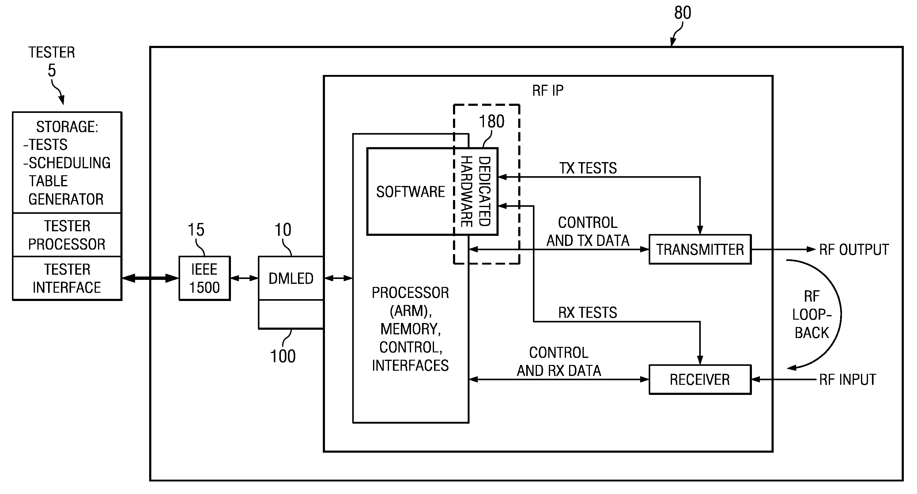
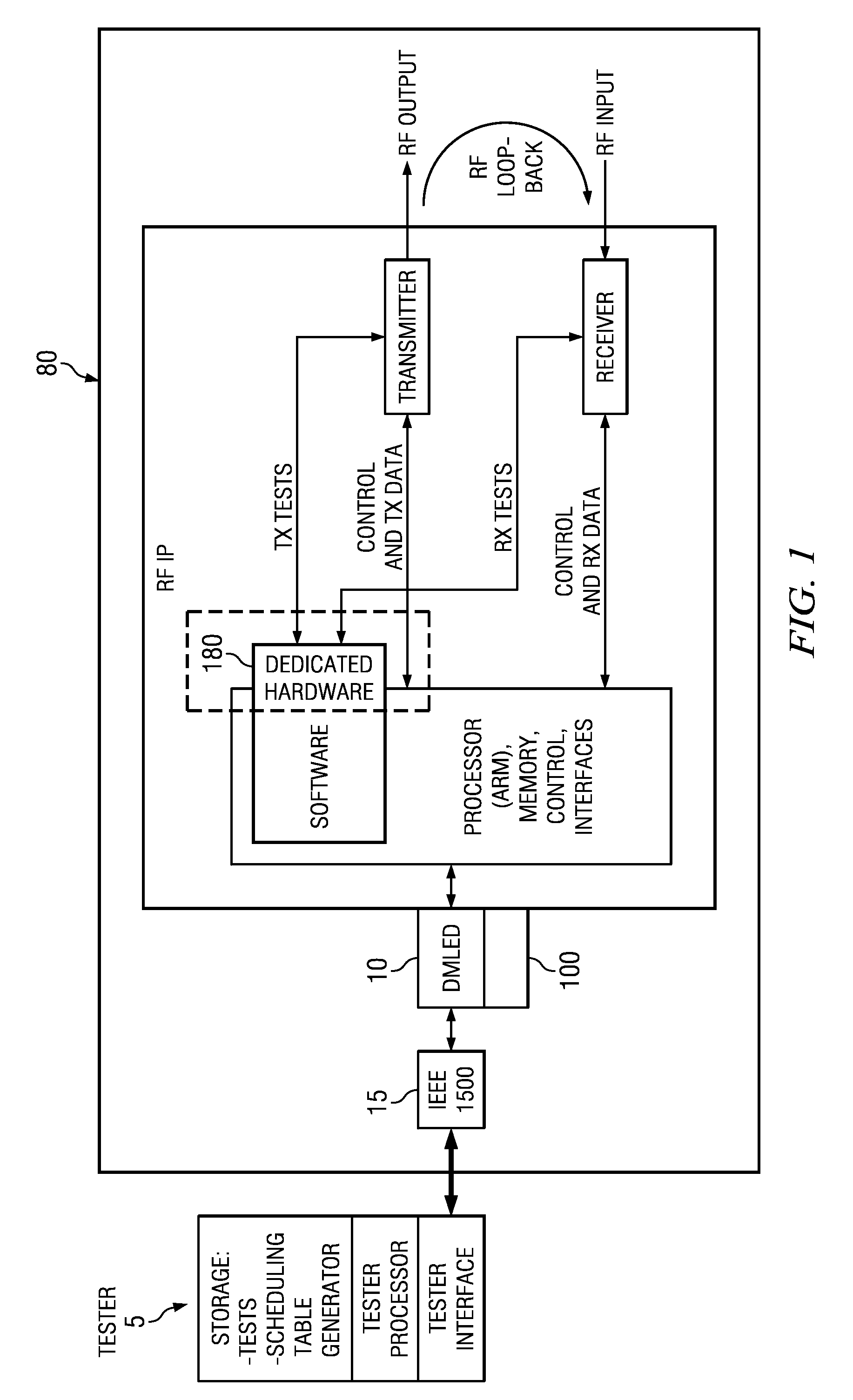
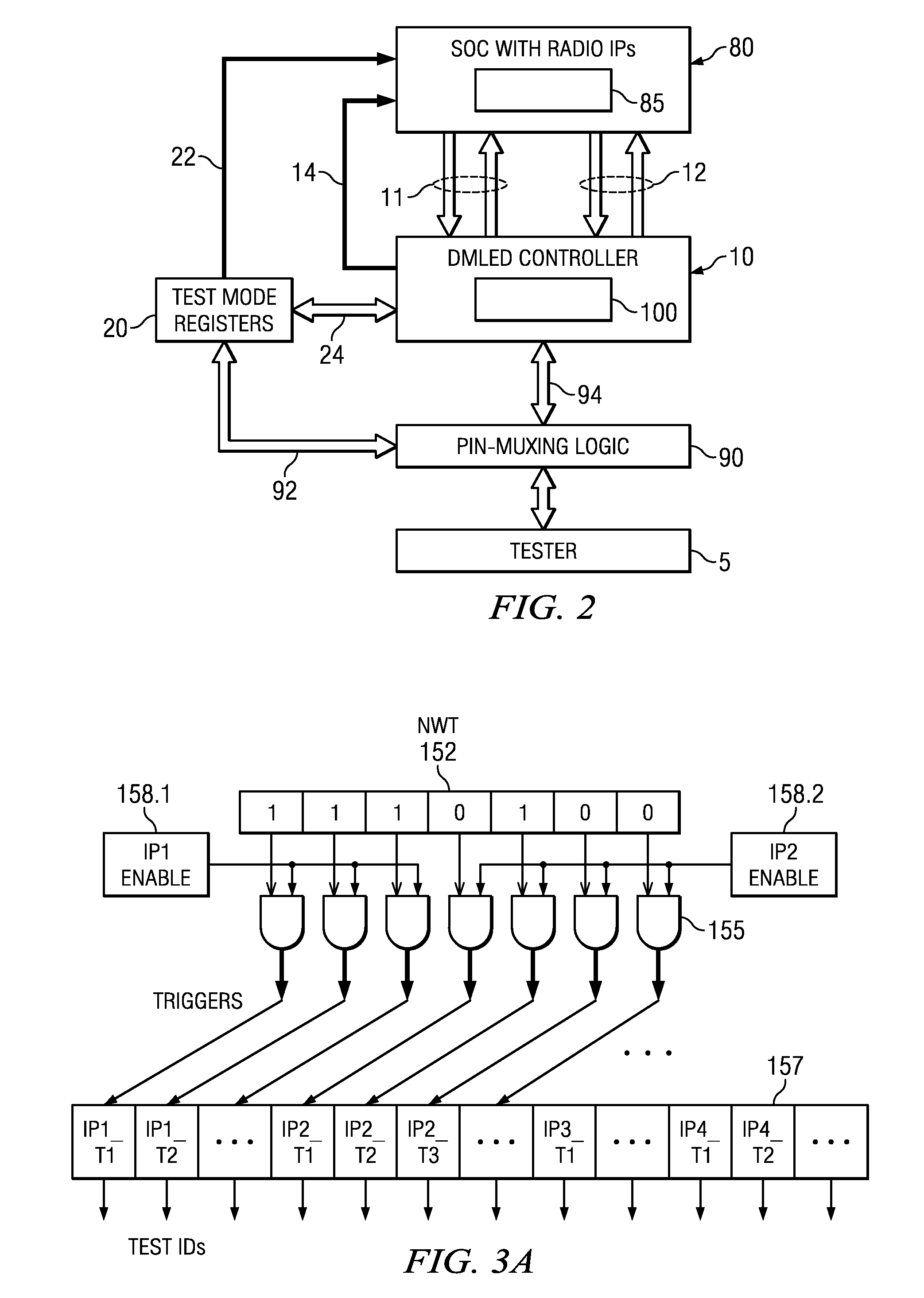
[0088]In FIGS. 1-3, a built-in self-test (BIST) controller embodiment 100 in a SOC 80 is used both for scheduling the tests for multiple RF modules and for actual test control 180 for the IP modules themselves. This provides the ability to create a dynamic test schedule structure that can be changed if required without having to less-efficiently re-create test vectors externally and apply them through the tester 5 and a test interface 15. Thus, hardware 100 is coupled with DMLED 10 and is implemented to run IP-specific tests simultaneously or concurrently on different IPs. Different tests, or sets of tests, are assigned unique Test IDs to which IP-specific control circuits 180 locally respond, and they can be selected and results of individual tests can be observed. Some embodiments provide a hardware scheduler 140 on-chip that permits and creates dynamic test execution schedules without the need to create distinct TDL (test description language of an external tester) sets for diffe...
embodiment 300
[0122]In FIG. 8, a combiner circuit embodiment 300 supports a DMLED circuit by providing an economical interface for many tests and signals. Combiner circuit 300 has AND gates 310.1-310.4 that each receive a pair of signal lines—a respective qualifying or masking line Cdr_XX_dmled test from a Core Data Register 360 of FIG. 9, and a corresponding line XX_dmled_test_exec that when active represents completion of execution of a test in a given IP core of FIG. 9. The placeholder symbolism XX represents wl: IP1 (WLAN), fm: IP2 (FM radio), bt: IP3 (Bluetooth), gps: IP4 (GPS satellite positioning receiver). A multi-input OR gate 320 is fed with the output from each of the AND gates 310.1-310.4. OR gate 320 output is coupled to the pin muxing logic 90 of FIGS. 2 and 9.
[0123]In FIG. 9, SOC 80 is fed from test pin mux circuit 90 with respective processor core Reset lines for the cores or sub-chips IP1-IP4 of SOC 80. A pad 350 carries signals to or from test pin mux circuit 90. Respective core...
embodiment 400
[0125]In FIG. 10, a process embodiment 400 for Test Sequencing has overlapping load and execute as in FIG. 12. Simultaneous execution commences once loading is done for all IPs for which tests are triggered. Pass and fail status results of the testing are observed at step 470 at the end. In FIG. 10, software-based serialized and / or concurrent RF testing involves functional tests on RF IP of FIG. 9. The tests are executed through DMLED (Direct Memory Load-Execute-Dump) operation controlled through ATE. Tests are loaded and results observed through DMLED interface 10 of FIGS. 1, 2, 9. Tests are executed on an embedded host processor on-chip that communicates with internal memory. Process steps or components of RF tests in FIG. 10 include:[0126]0) Wafer / dice fabrication 410.[0127]1) Initialization 415 (power-up, E-Fuse shift, PLL lock for all IPs in parallel, ROM / RAM boot up 420 for all IPs for which tests are triggered by controller 100).[0128]2) Firmware (FW) download+execution time....
PUM
 Abstract
Description
Claims
Application Information