Chemical mechanical polishing method

Inactive Publication Date: 2012-08-02
SEMICON MFG INT (SHANGHAI) CORP
View PDF8 Cites 3 Cited by
  • Summary
  • Abstract
  • Description
  • Claims
  • Application Information

AI Technical Summary

Benefits of technology

[0025]In another embodiment, while the surface of the dielectric layer is cleaned by the alkaline solution, the pressure on the wafer of the grinding head is set to be lower than th

Problems solved by technology
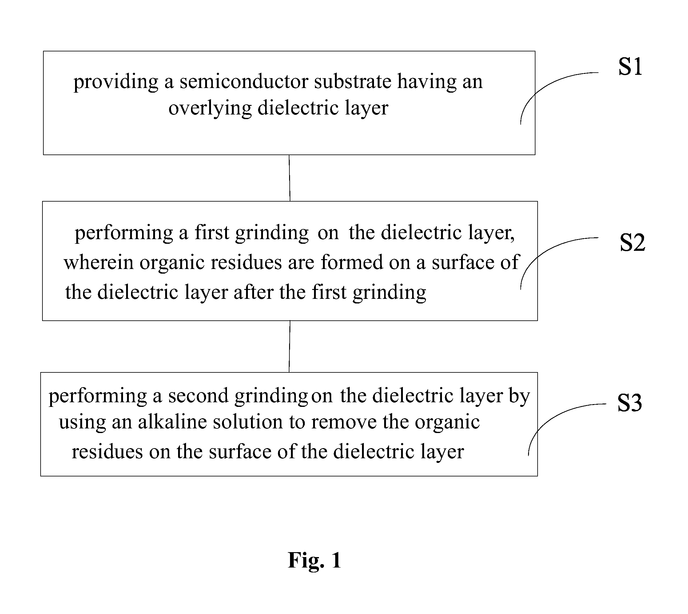
When a dielectric layer is grinded according to a conventional method, the surface of the wafer is abraded by grinding particles in oxidation grinding solution, which may cause scratches on the wafer surface.
And organic residues may be produced by chemical additives in the grinding soluti

Method used


Image

  • Chemical mechanical polishing method
  • Chemical mechanical polishing method
  • Chemical mechanical polishing method

Examples


Embodiment Construction

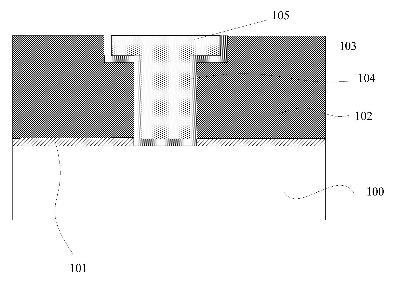
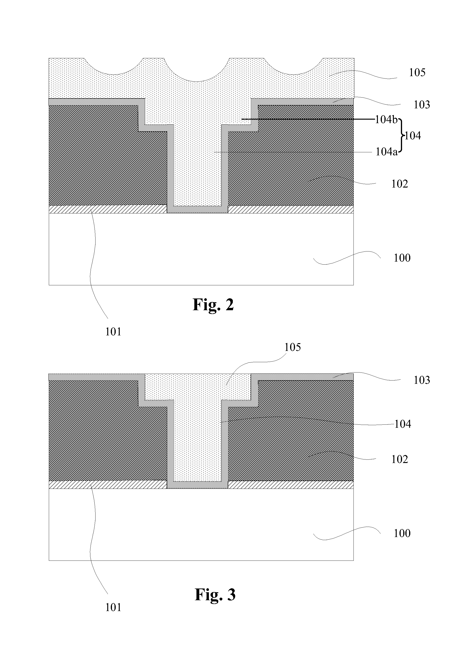
[0029]A conventional CMP process uses a surfactant to remove organic residues remaining on a surface of a substrate or wafer. However, a large amount of residues is remaining on the surface of the substrate or wafer after cleaning the surface using a surfactant. As known to one of ordinary skill in the art, a surfactant is a type of stable bipolar micelle with both hydrophilic and hydrophobic properties, which may be arranged according to certain orientation on a solution surface and significantly reduce a surface tension thereof. Specifically, the organic residues are made of hydrophobic materials, such as copper inhibitors, BTA, and the like, most of which are water-insoluble. Therefore, when the surfactant contacts with the organic residues, because of a presence of the hydrophobic micelle, a repulsive force is much larger than an attraction force between the surfactant and the water molecules. Therefore, the surfactant molecules assemble on surfaces of the organic residues accor...


PUM


Abstract

A Chemical Mechanical Polishing (CMP) method includes providing a semiconductor substrate having an overlying dielectric layer, performing a first grinding on the dielectric layer, wherein the first grinding produces organic residues on a surface of the dielectric layer after the first grinding. The method further includes performing a second grinding on the dielectric layer by using an alkaline solution to remove the organic residues on the surface of the dielectric layer. The organic residues remaining on the surface of the dielectric layer are removed by using the alkaline solution after the first grinding process is performed. The method additionally includes cleaning a grinding pad and the substrate using deionized water.

Description

CROSS-REFERENCES TO RELATED APPLICATIONS[0001]The present application claims the priority of Chinese Patent Application No. 201110211074.6, entitled “CHEMICAL MECHANICAL POLISHING METHOD”, filed on Jul. 26, 2011, which claims the priority of Chinese Patent Application No. 201110034148.3, entitled “CHEMICAL MECHANICAL POLISHING METHOD”, and filed on Jan. 31, 2011, the entire disclosures of which are incorporated herein by reference.FIELD OF THE INVENTION[0002]The present invention generally relates to semiconductor manufacture technology, and more particularly, to a chemical mechanical polishing method of planarizing a dielectric layer and removing organic residues remaining on the surface of the planarized dielectric layer.BACKGROUND OF THE INVENTION[0003]In semiconductor technology, Chemical Mechanical Polishing (CMP) technology uses two types of grinding, a mechanical grinding and a chemical grinding, to planarize a wafer or a semiconductor layer. A flat surface of wafer or semico...

Claims


Application Information

Patent Timeline
IPC IPC(8): H01L21/306
CPCH01L21/02074H01L21/31053H01L21/7684H01L21/76819H01L21/3212
Inventor DENG, WUFENG
Owner SEMICON MFG INT (SHANGHAI) CORP
Why Eureka
Try Eureka