


Quick Research
Generate reliable direction feasibility study reports for your R&D in just a few steps.

Technical Q&A
Discover and master advanced knowledge NOW. Basics, ideas, possibilities, all at once.

Find Solutions
As an expert in R&D theories, this can generate solutions to your technical problems instantly.

Evaluate Feasibility
Analyze your overall solution with one click, know your potential R&D risks in advance.

Monitor Landscape
Get weekly tech updates, stay abreast of the latest tech innovations and key insights.
BSI image sensor package with variable light transmission for even reception of different wavelengths
- Summary
- Abstract
- Description
- Claims
- Application Information
AI Technical Summary
Benefits of technology
Problems solved by technology
Method used
Image

Examples
second embodiment
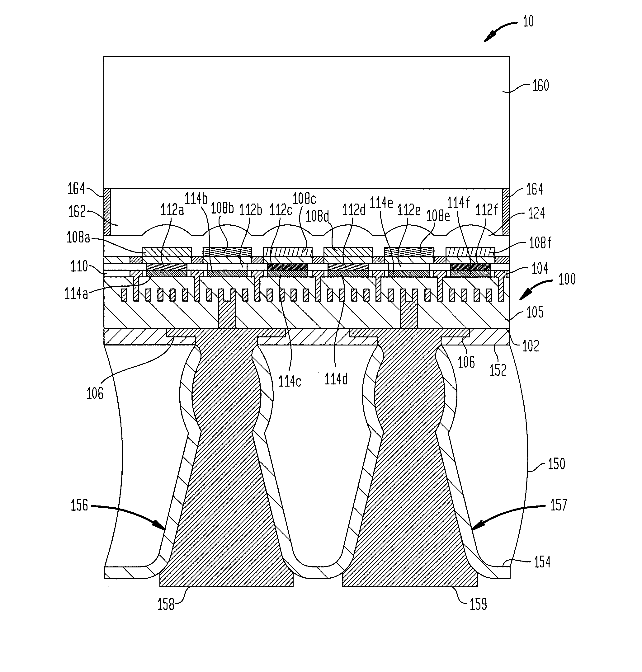
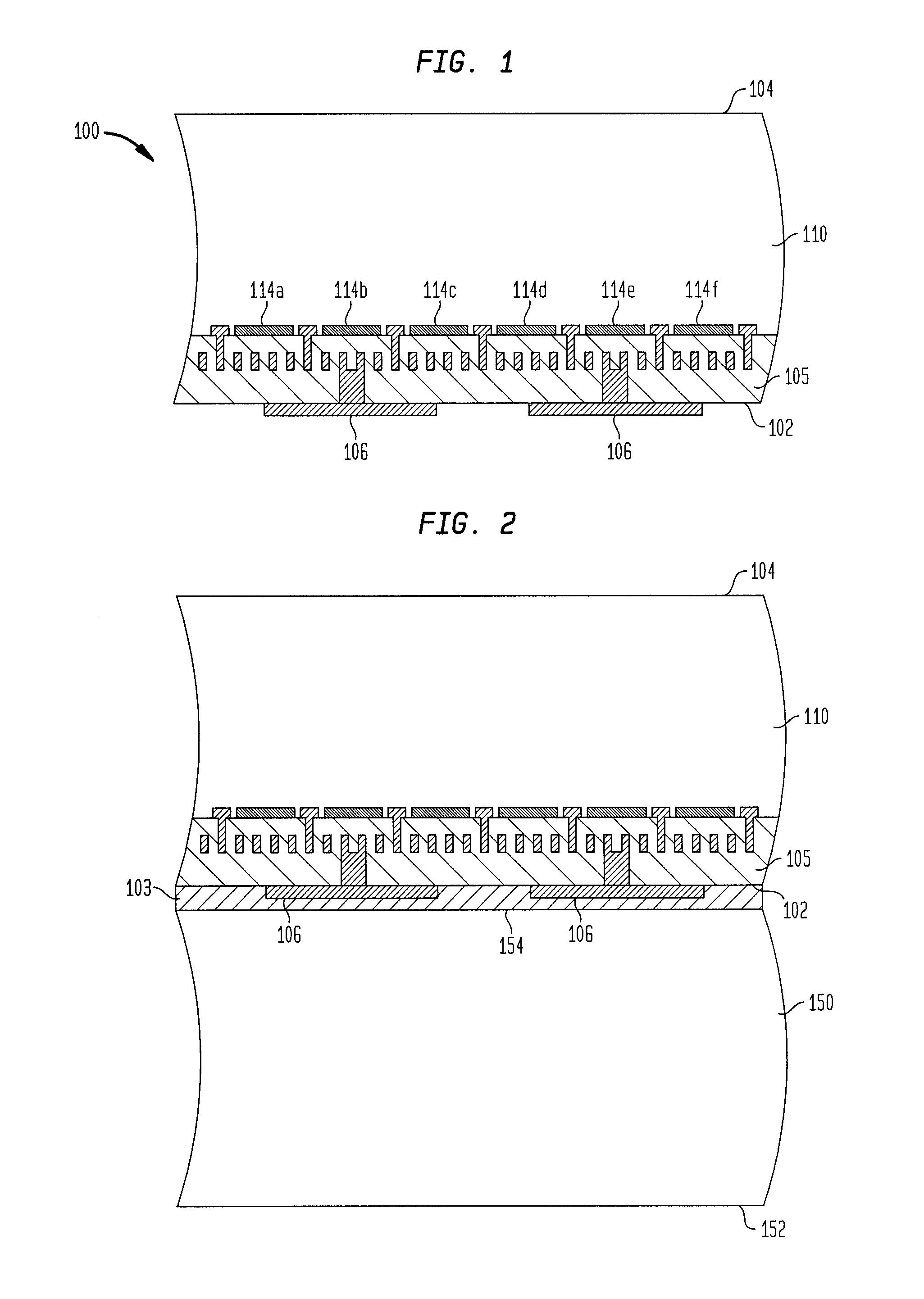
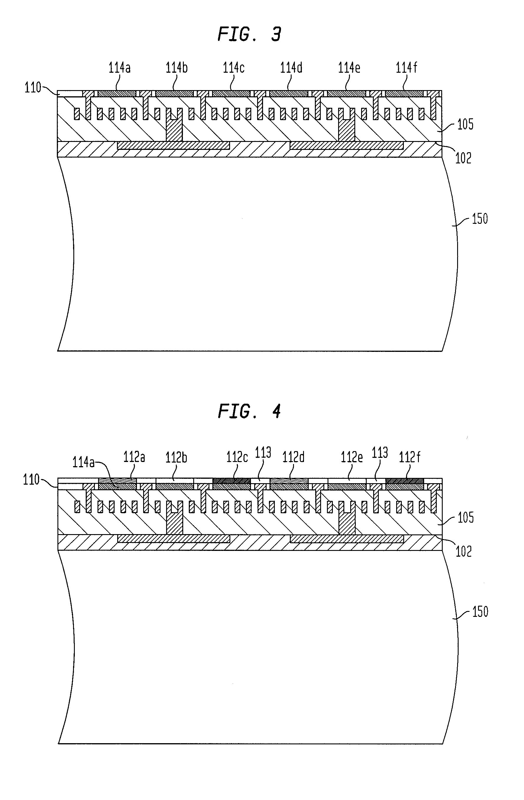
[0038]FIG. 8 depicts a microelectronic image sensor assembly 20 according to the present invention. Assembly 20 is similar in nearly all respects as assembly 10 as described above. However, the main difference is that areas 112 of different reflectivities are replaced with different materials 212a-f having different light transmission properties defined by fillers present in each material 212. Such fillers may differ by particle size, density, and / or type, and each material 212 may have a different surface finish. Between neighboring individual areas 212, e.g., areas 212a, 212b, filler areas 213 may be provided. The filler areas 213 may have even greater absorption values as one or more of the areas 212a, 212b, etc. described above. It may not necessary to include a metal grid in connection with assembly 20. Further, assembly 20 may include an antireflective coating 220 overlying semiconductor region 210, antireflective coating 220 separating the semiconductor region 210 from areas ...
third embodiment
[0039]FIG. 9 depicts a microelectronic image sensor assembly 30 according to the present invention. Assembly 20 is similar in nearly all respects as assembly 10 as described above. However, the main difference is that areas 112 of different reflectivities are replaced with regions 312a-f of material having a high refractive index that are patterned to different thickness, such that the intensity of light transmitted to respective LSEs 314a, 314b, 314c is the same or approximately the same. The thickness of each region 312a-f above the rear face 304 can be determined according to the properties of the material used for each region 312. In one embodiment, the same material can be used for each of the six regions 312a-f illustrated in FIG. 9. In this case, the thickness of each of the regions 312 in a direction away from the respective LSE 314 over which such region 312 lies can be selected such that the product of the light absorption in each region 312 and the light absorption in the...
PUM
 Abstract
Description
Claims
Application Information
 - R&D Engineer
- R&D Manager
- IP Professional
- Industry Leading Data Capabilities
- Powerful AI technology
- Patent DNA Extraction
Browse by: Latest US Patents, China's latest patents, Technical Efficacy Thesaurus, Application Domain, Technology Topic, Popular Technical Reports.
© 2024 PatSnap. All rights reserved.Legal|Privacy policy|Modern Slavery Act Transparency Statement|Sitemap|About US| Contact US: help@patsnap.com