Avalanche impact ionization amplification devices
a technology of avalanche impact and ionization, which is applied in the field of avalanche amplification photodetectors and avalanche impact ionization transistors, can solve the problems of bulky, expensive manufacture, and high cost of current amplification in semiconductor devices, and achieves the effect of reducing the cost of current amplification
- Summary
- Abstract
- Description
- Claims
- Application Information
AI Technical Summary
Problems solved by technology
Method used
Image

Examples
first embodiment
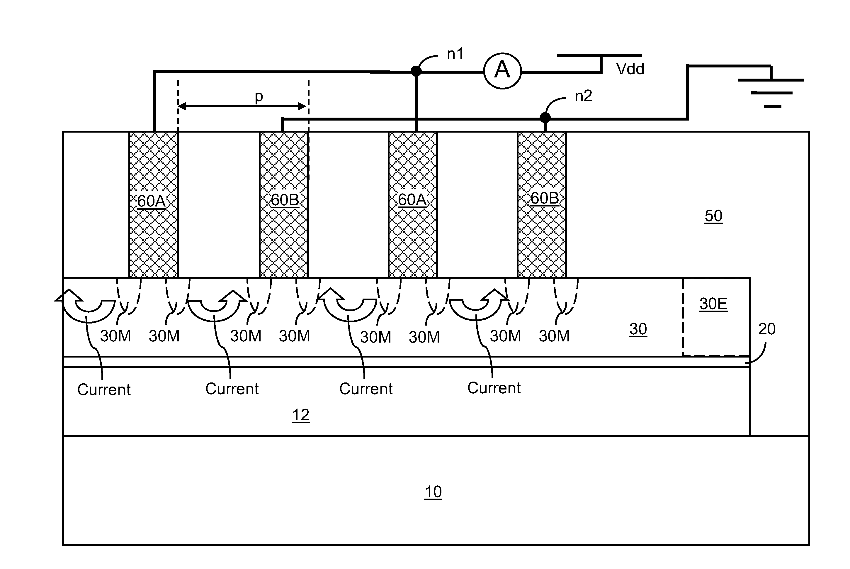
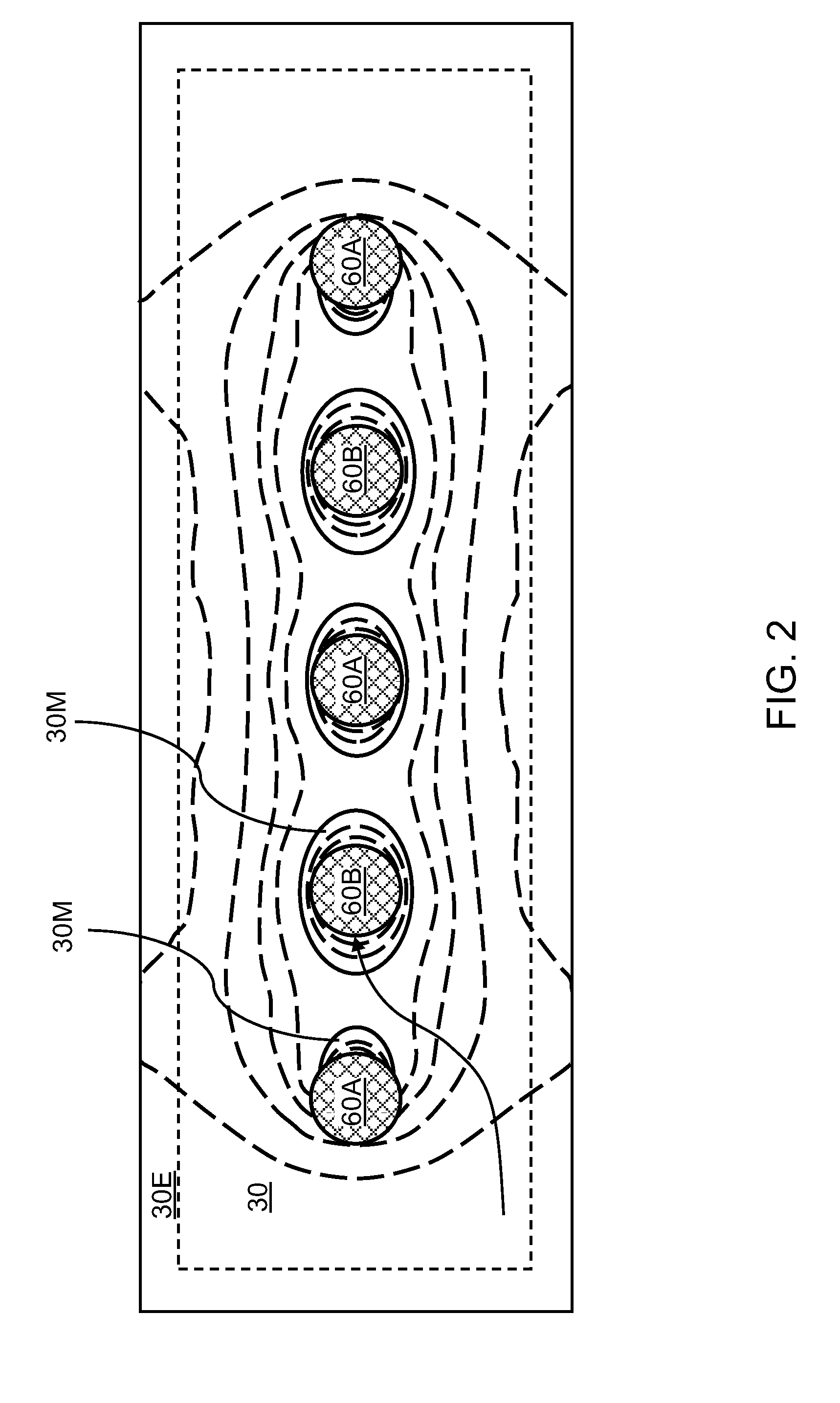
[0025]Referring to FIG. 1, a first exemplary semiconductor structure according to the present invention includes a substrate 10, a waveguide 12 located on a top surface of the substrate 10, a dielectric material layer 20 located on a top surface of the waveguide 12, a semiconductor material layer 30 located on the substrate 10 and above the waveguide 12, an overlying dielectric material layer 50 located above the semiconductor material layer 30, at least one first-type electrode 60A located in proximity to, e.g., over a top surface of, the semiconductor material layer 30 and embedded in the overlying dielectric material layer 50, and at least one second-type electrode 60B located in proximity to, e.g., over the top surface of, the semiconductor material layer 30 and embedded in the overlying dielectric material layer 50. The at least one first-type electrode 60A and at least one second-type electrode 60B are conductively connected to the semiconductor material layer 30. The resistan...
second embodiment
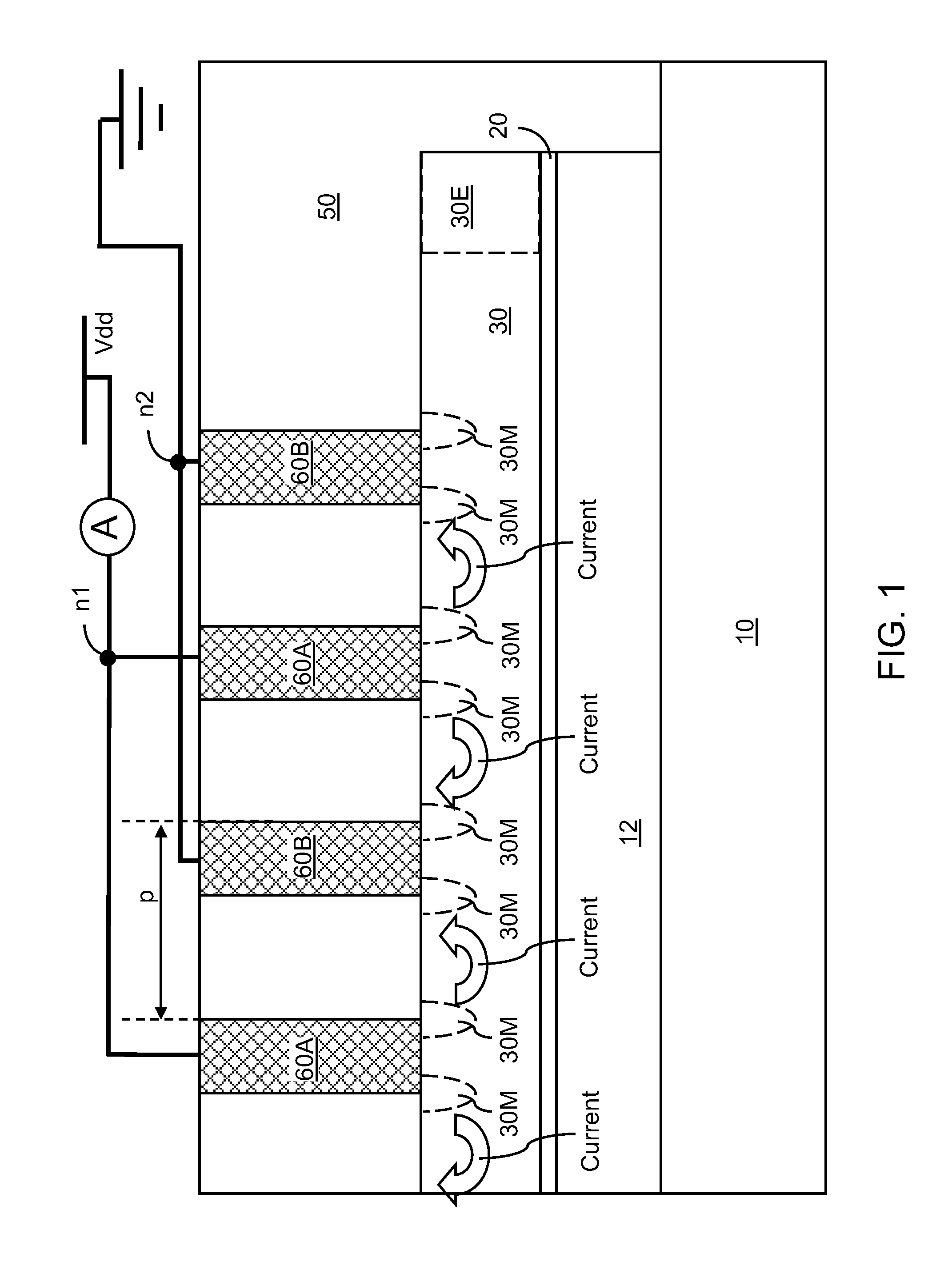
[0052]Referring to FIG. 3, a second exemplary semiconductor structure according to the present invention is derived by removing the waveguide 12 from the first exemplary semiconductor structure. In this case, electromagnetic radiation impinges through the overlying dielectric material layer 50 of the substrate 10 and the dielectric material layer 20.
[0053]In one embodiment, the overlying dielectric material layer 50 is an optically transparent material such as silicon oxide, and photons in electromagnetic radiation propagate through the overlying dielectric material layer 50 onto the semiconductor material layer 30. In another embodiment, the substrate 10 and the dielectric material layer 20 are optically transparent material such as silicon dioxide, and photons in electromagnetic radiation propagates through the substrate 10 and the dielectric material layer 20. The optically transparent material does not absorb electromagnetic radiation over at least a portion of the wavelength ra...
third embodiment
[0054]Referring to FIG. 4, a third exemplary semiconductor structure according to the present invention is derived from the first or second exemplary semiconductor structure by forming a thin material liner 40 directly on the top surface of the semiconductor material layer 30. The thin material liner 40 contacts the bottom surface of each of the at least one first-type electrode 60A and the at least one second-type electrode 60B. The thin material liner 40 vertically separates the semiconductor material layer 30 from each of the at least one first-type electrode 60A and the at least one second-type electrode 60B. The overlying dielectric material layer 50 contacts the top surface of the thin material liner 40.
[0055]The thin material liner 40 has a dielectric material that unpins the Fermi level at the surface of the semiconductor material layer 30. The unpinning of the Fermi level reduces the dark current, which is a steady state current that flows between the at least one first-typ...
PUM
 Abstract
Description
Claims
Application Information
 - R&D
- Intellectual Property
- Life Sciences
- Materials
- Tech Scout
- Unparalleled Data Quality
- Higher Quality Content
- 60% Fewer Hallucinations
Browse by: Latest US Patents, China's latest patents, Technical Efficacy Thesaurus, Application Domain, Technology Topic, Popular Technical Reports.
© 2025 PatSnap. All rights reserved.Legal|Privacy policy|Modern Slavery Act Transparency Statement|Sitemap|About US| Contact US: help@patsnap.com