Solid-state imaging apparatus
- Summary
- Abstract
- Description
- Claims
- Application Information
AI Technical Summary
Benefits of technology
Problems solved by technology
Method used
Image
Examples
first embodiment
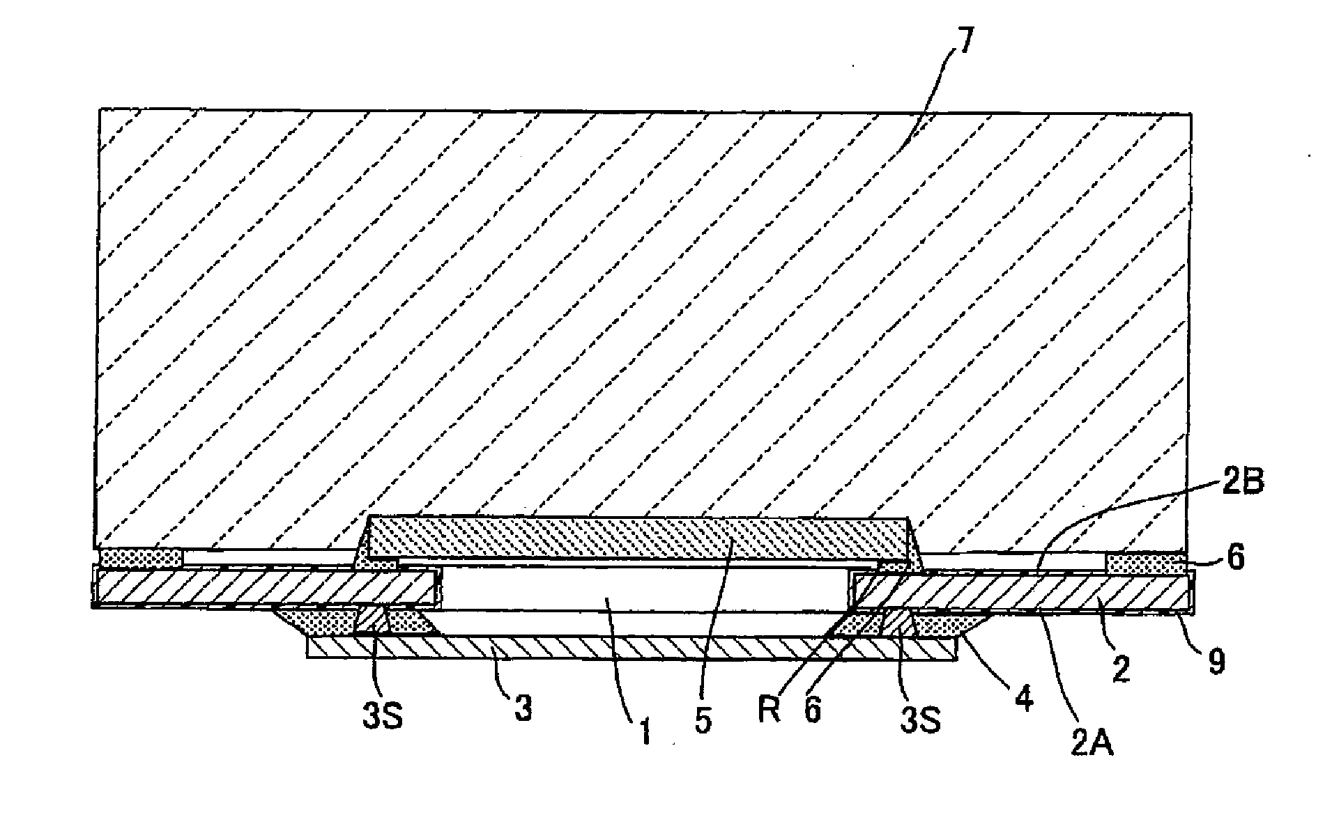
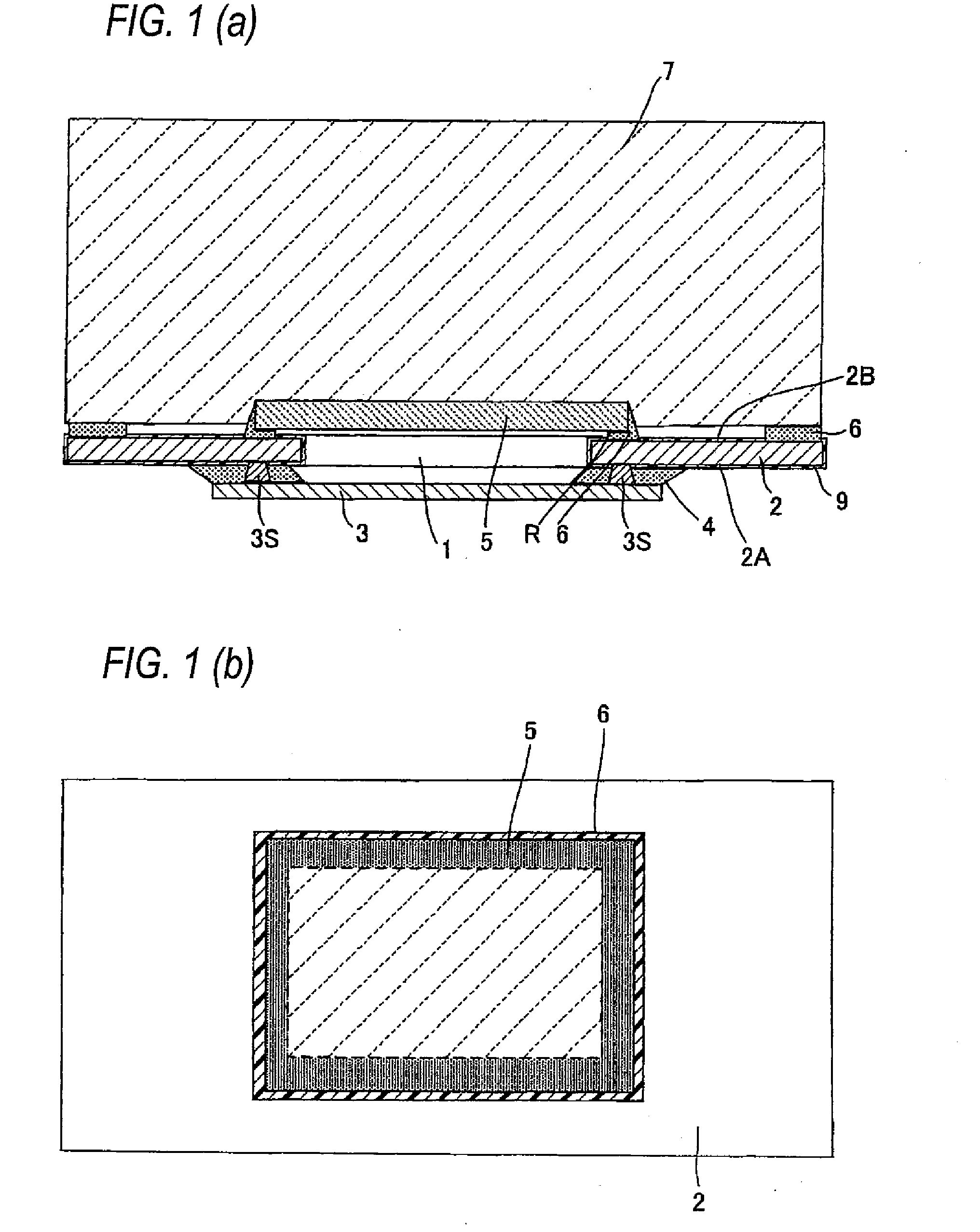
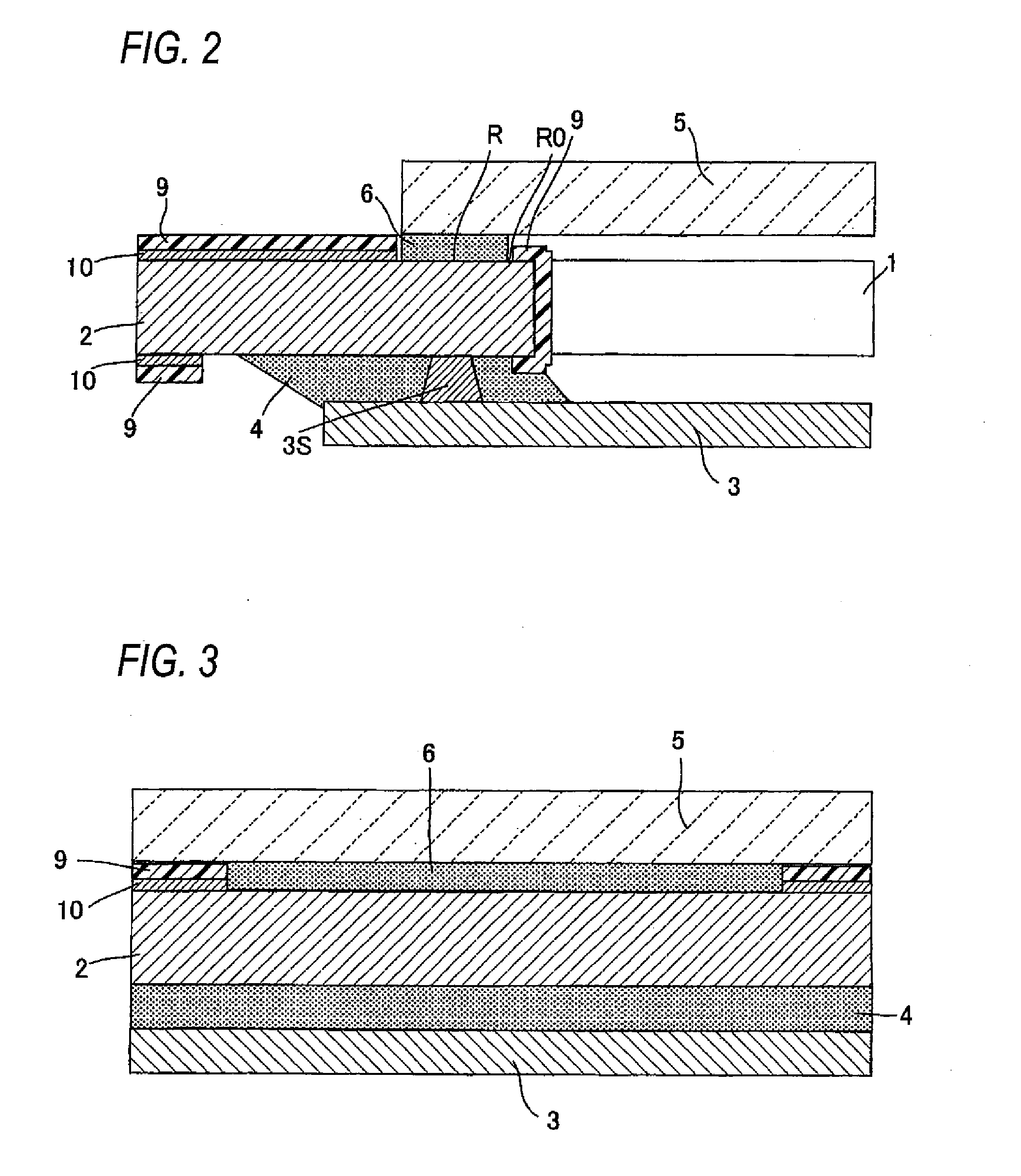
[0028]FIGS. 1(a) to 3 show a solid-state imaging apparatus of a first embodiment of the invention. FIG. 1(a) is a schematic sectional view and FIG. 1(b) is a top view of this solid-state imaging apparatus, and FIG. 2 is a main enlarged view of FIG. 1(a), and FIG. 3 is a further main enlarged view of FIG. 2. FIGS. 4(a) to 4(c) are diagrams showing a manufacturing step of a structural body of this solid-state imaging apparatus.
[0029]This solid-state imaging apparatus includes an insulating structural body 2 having a through opening 1, a wiring part 10 formed on a front surface of this structural body 2, a solid-state imaging element 3 which is connected to the wiring part 10 and also is attached to the structural body 2 so as to close the through opening 1, a translucent member 5 which is opposed to the solid-state imaging element 3 and is attached to the structural body 2 through an adhesive 6 inside an adhesion region R so as to close the through opening 1, and a solder resist film ...
second embodiment
[0056]Next, a second embodiment of the invention will be described.
[0057]FIGS. 5(a), 5(b), and 6 show a solid-state imaging apparatus of the second embodiment of the invention. FIG. 5(a) is a schematic sectional view and FIG. 5(b) is a top view of this solid-state imaging apparatus. FIG. 5(a) is a sectional view taken on line A-A of FIG. 5(b).
[0058]The present embodiment is characterized in that a shape of a region R0 in which a solder resist is removed is adjusted so as to have an air escape part 11 as a communication region in which space of a through opening 1 communicates with the outside air. In the embodiment, the space of the through opening 1 generated by arranging a solid-state imaging element 3 and a translucent member 5 in a state of sandwiching a structural body 2 from both sides communicates with the outside air through the air escape part 11 provided by a situation in which an adhesive 6 is not supplied partially, and air can enter and exit freely and thereby, a config...
third embodiment
[0069]Next, a third embodiment of the invention will be described.
[0070]FIGS. 7(a) and 7(b) show a solid-state imaging apparatus of the third embodiment of the invention. FIG. 7(a) is a main enlarged schematic sectional view and FIG. 7(b) is a top view of this solid-state imaging apparatus.
[0071]The present embodiment is an example of modifying the air escape part 11 in the second embodiment and is configured to form a dust trap pocket 12 inside the air escape part 11 in at least one place by providing a laminated structure of a solder resist film 9 and a wiring part 10 in at least one place so that the air escape part 11 has a relation of intersecting with an airflow direction. Also in this example, a film thickness of an adhesive 6 is constructed so as to become thicker than that of the solder resist film 9 and a region sandwiched in a region R0 in which the solder resist film 9 is removed constructs the air escape part 11 as shown by a broken line. This air escape part 11 is a ga...
PUM
 Abstract
Description
Claims
Application Information


