
Variable wavelength interference filter, optical module, and optical analysis device

a wavelength interference filter and variable wavelength technology, applied in the direction of optics, optical elements, instruments, etc., can solve the problems of difficult wiring operation, inability to easily and reliably connect the bonding pads electrically to each other, etc., and achieve the effect of accurate spectral characteristics and high accuracy

Active Publication Date: 2012-08-16
SEIKO EPSON CORP
View PDF2 Cites 22 Cited by
  • Summary
  • Abstract
  • Description
  • Claims
  • Application Information

AI Technical Summary

Benefits of technology

[0009]An advantage of some aspects of the invention is to provide a variable wavelength interference filter, an optical module, and an optical analysis device for making it possible to electrically connect the electrodes to each other with an easy and simple operation.

Problems solved by technology

However, since the extraction electrodes are respectively disposed on the surfaces of the pair of substrates, the surfaces being opposed to each other, there is a problem that the wiring operation becomes difficult.
However, in the variable shape mirror described in Document 1 mentioned above, it is required to separately dispose electrically conductive intermediate members such as Au bumps in order to electrically connecting the mirror substrate-side bonding pads and the wiring substrate-side bonding pads, and there is a problem that it is not achievable to easily and reliably make these bonding pads electrically be connected to each other.

Method used


Image

  • Variable wavelength interference filter, optical module, and optical analysis device
  • Variable wavelength interference filter, optical module, and optical analysis device
  • Variable wavelength interference filter, optical module, and optical analysis device

Examples


first embodiment

[0046]A first embodiment of the invention will hereinafter be explained with reference to the accompanying drawings.

1. Schematic Configuration of Colorimetric Device

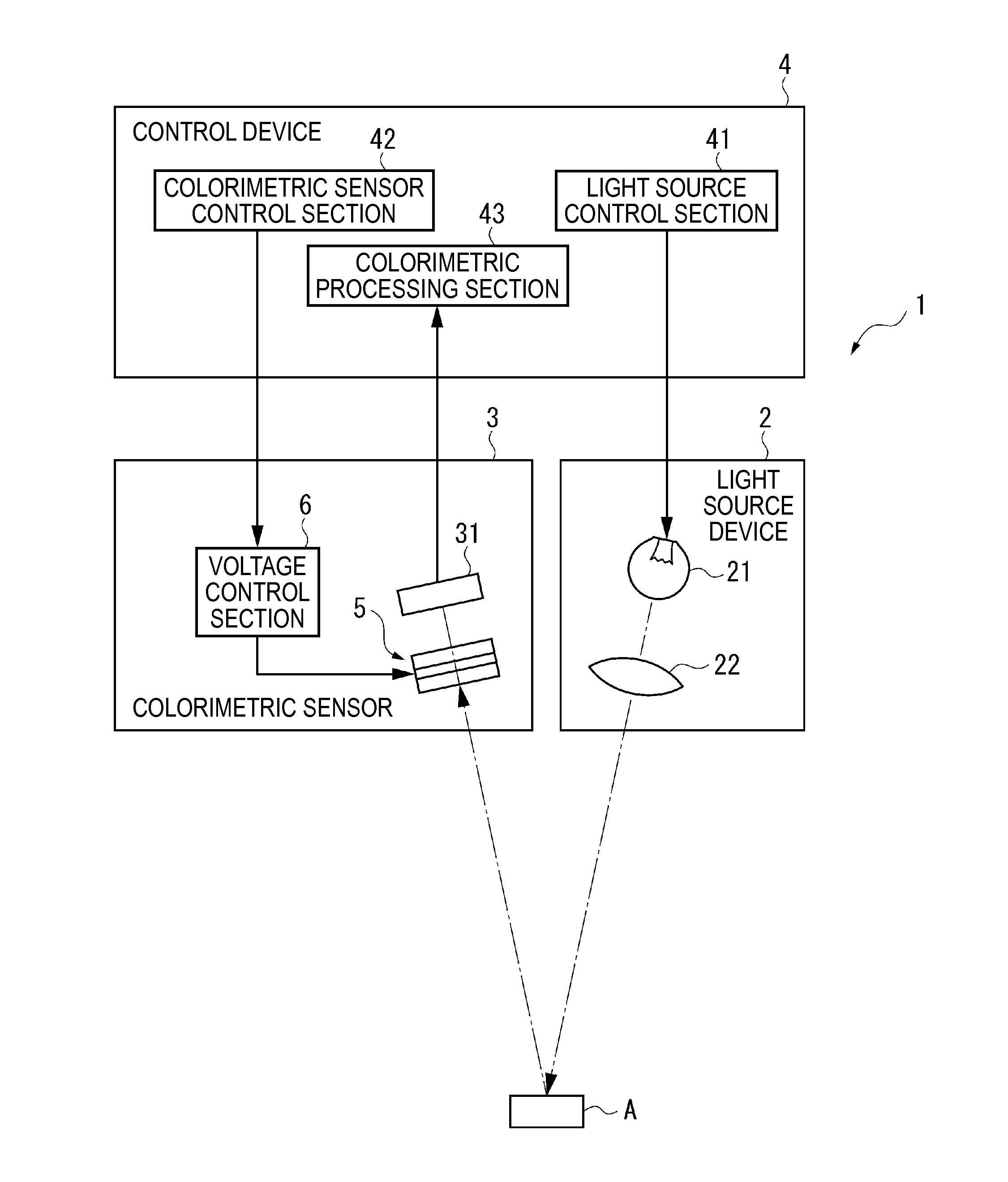
[0047]FIG. 1 is a block diagram showing a schematic configuration of a colorimetric device 1 (an optical analysis device) according to the present embodiment.

[0048]As shown in FIG. 1, the colorimetric device 1 is provided with a light source device 2 for emitting light to a test object A, a colorimetric sensor 3 (an optical module), and a control device 4 for controlling an overall operation of the colorimetric device 1. Further, the colorimetric device 1 is a device for making the light, which is emitted from the light source device 2, be reflected by the test object A, receiving the test target light thus reflected using the colorimetric sensor 3, and analyzing and then measuring the chromaticity of the test target light, namely the color of the test object A, based on the detection signal output from the colorimetric ...

second embodiment

[0127]A second embodiment according to the invention will hereinafter be explained with reference to FIGS. 9 and 10.

[0128]FIG. 9 is a schematic cross-sectional view of the etalon 5A according to the present embodiment in a condition of being housed in a housing chassis 7, and FIG. 10 is a schematic cross-sectional view showing the etalon 5A before housed in the housing chassis 7.

[0129]It should be noted that in the following explanation the constituents identical to those of the first embodiment will be denoted by the same reference symbols, and the explanation therefor will be omitted.

[0130]The colorimetric sensor 3A according to the present embodiment is provided with the housing chassis 7 besides the light receiving element 31 (see FIG. 1), the voltage control section 6 (see FIG. 1), and the etalon 5A.

[0131]The movable substrate 52 of the etalon 5A is provided with a groove section 527 formed at a position corresponding to the second electrode surface 525. Therefore, since a thin...


PUM

PropertyMeasurementUnit
thicknessaaaaaaaaaa
thicknessaaaaaaaaaa
surface roughnessaaaaaaaaaa

Abstract

An etalon is provided with a fixed substrate and a movable substrate opposed to the fixed substrate. The fixed substrate is provided with a first bonding surface to be bonded to the movable substrate via a bonding film and a first electrode surface on which a part of the first electrode is formed. The movable substrate is provided with a second bonding surface to be bonded to the first bonding surface via the bonding film and a second electrode surface on which a part of the second electrode is formed. In the state in which the fixed substrate and the movable substrate are bonded to each other with the bonding film, the first electrode formed on the first electrode surface and the second electrode formed on the second electrode surface have contact with each other.

Description

BACKGROUND[0001]1. Technical Field[0002]The present invention relates to a variable wavelength interference filter, an optical module equipped with the variable wavelength interference filter, and an optical analysis device equipped with the optical module.[0003]2. Related Art[0004]In the past, there has been known a variable wavelength interference filter having reflecting films respectively disposed on surfaces of a pair of substrates, the surfaces being opposed to each other, so as to opposed to each other via a predetermined gap, and drive electrodes respectively disposed on the surfaces of the substrates, the surfaces being opposed to each other. In such a variable wavelength interference filter, a voltage is applied between the drive electrodes to thereby control the gap between the reflecting films using the electrostatic force.[0005]In such a variable wavelength interference filter, it is required to form an extraction electrode, which extends from each of the drive electrod...

Claims


Application Information

Patent Timeline
Patent Type & Authority Applications(United States)
IPC IPC(8): G02B5/28G01B9/02G01J3/26G01J3/50G01N21/00G01N21/35G01N21/3504G01N21/359G02B26/00
CPCG01J3/26G02B26/001H01L27/14621G01J3/51G01J3/50G01N21/25
Inventor SANO, AKIRAHIROKUBO, NOZOMU
Owner SEIKO EPSON CORP
Features
  • Generate Ideas
  • Intellectual Property
  • Life Sciences
  • Materials
  • Tech Scout
  • Unparalleled Data Quality
  • Higher Quality Content
  • 60% Fewer Hallucinations
Learn More