Semiconductor device and method of manufacturing the same

a technology of semiconductors and semiconductors, applied in the direction of semiconductor devices, electrical equipment, transistors, etc., can solve the problems of increasing the capacity of drams that will likely reach the limit, and achieve the effects of improving processing margin, reducing contact resistance, and increasing the etching width of storage nodes

Active Publication Date: 2012-08-23
SK HYNIX INC
View PDF2 Cites 16 Cited by
  • Summary
  • Abstract
  • Description
  • Claims
  • Application Information

AI Technical Summary

Benefits of technology

[0009]Embodiments of the present invention are directed to providing a semiconductor device having relatively low contact resistance. In an embodiment, an isolation pattern is formed on a device isolation structure and contact plugs are formed at sides of the isolation pattern so that a full overlap between a storage node contact and an active region is provided to solve an overlay in an etching process, and an etching width of a storage node is increased to improve processing margin.
[0010]According to one aspect of an exemplary embodiment, a semiconductor device includes a main gate and a device isolation structure disposed in a semiconductor substrate, an isolation pattern disposed on the device isolation structure, and contact plugs disposed at sides of the isolation pattern. The isolation pattern is formed on the device isolation structure and the contact plugs are formed at sides of the isolation pattern so that a full overlap between a storage node contact and an active region is provided to solve an overlay in an etching process and an etching line width of a storage electrode to provide a processing margin.
[0014]The isolation pattern may be formed so that a lower portion of the isolation pattern is buried within an upper portion of the recess to prevent the isolation pattern from collapsing.
[0018]According to another aspect of another exemplary embodiment, a semiconductor device includes an active region formed in a line type in a semiconductor substrate, a main gate obliquely extending to the active region, an isolation gate in the semiconductor substrate, an isolation pattern of a line type disposed on the isolation gate, and contact plugs extending along both sides of the isolation pattern. The isolation pattern is formed on a device isolation structure and contact plugs are formed at both sides of the isolation pattern. Thereby, a full overlap between a storage node contact and the active region is provided to improve an overlay in an etching process and an etching line width of a storage node is increased to improve a processing margin.
[0023]According to another aspect of another exemplary embodiment, a method of manufacturing a semiconductor device includes forming a main gate and a device isolation structure in a semiconductor substrate, forming an isolation pattern on the device isolation structure, and forming contact plugs at the both sides of the isolation pattern. The isolation pattern is formed on the device isolation structure and contact plugs are formed at both sides of the isolation pattern. Thereby, a full overlap between a storage node contact and an active region is provided to improve an overlay in an etching process and an etching line width of a storage node is increased to improve a processing margin.

Problems solved by technology

Recently, although demand for large capacity of semiconductor memory devices, particularly dynamic random access memories (DRAMs), has increased, increases in capacity of DRAMs will likely reach the limit in the near future as the DRAM technology goes down below 30 nm due to the difficulty of making functioning DRAM cells with the feature size that is significantly less than 30 nm.
One challenge of implementing the buried gate structure technology is the relatively small contact area between a storage node contact and an active region.

Method used


Image

  • Semiconductor device and method of manufacturing the same
  • Semiconductor device and method of manufacturing the same
  • Semiconductor device and method of manufacturing the same

Examples


Embodiment Construction

.”

BRIEF DESCRIPTION OF THE DRAWINGS

[0041]The above and other aspects, features, and other advantages of the subject matter of the present disclosure will be more clearly understood from the following detailed description taken in conjunction with the accompanying drawings, in which:

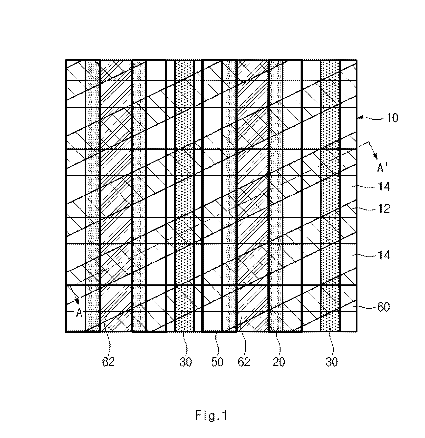
[0042]FIG. 1 is a plan view of a semiconductor device according to an embodiment of the present invention.

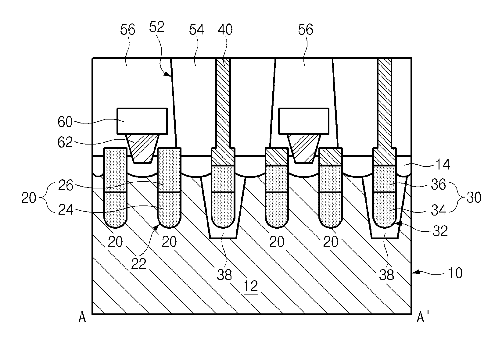
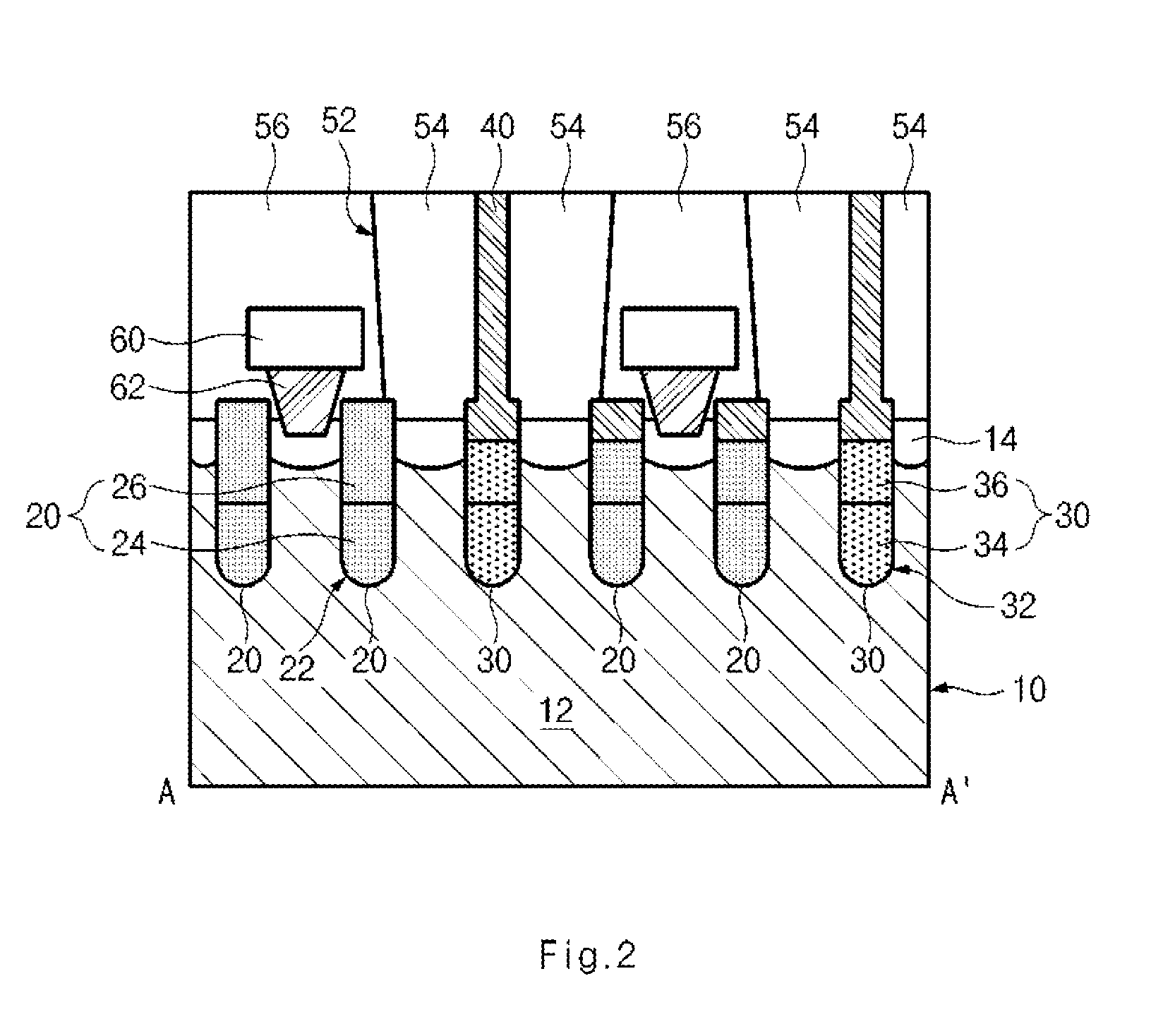
[0043]FIG. 2 is a cross-sectional view of the semiconductor device taken along the line A-A′ of FIG. 1.

[0044]FIGS. 3 through 14 are cross-sectional views illustrating a method of manufacturing the semiconductor device according to an embodiment of the present invention, which are taken along the line A-A′; and

[0045]FIG. 15 is a cross-sectional view of a semiconductor device according to another embodiment of the present invention.

DESCRIPTION OF EXEMPLARY EMBODIMENT

[0046]Exemplary embodiments are described herein with reference to cross-sectional illustrations that are schematic illustrations of exempl...


PUM


Abstract

A semiconductor device and a method of fabricating the same are provided, in which a full overlap between a storage node contact and an active region to solve an overlay in an etching process and an etching width of a storage node is increased to improve a processing margin. The semiconductor device includes a main gate and a device isolation structure disposed in a semiconductor device, an isolation pattern disposed over the device isolation structure, and contact plugs disposed at each side of the isolation pattern.

Description

CROSS-REFERENCES TO RELATED APPLICATION[0001]This application claims priority under 35 U.S.C. 119(a) to Korean application number 10-2011-0015619, filed on 22 Feb. 2011, in the Korean Patent Office, which is incorporated by reference in its entirety to this application.BACKGROUND OF THE INVENTION[0002]1. Technical Field[0003]Embodiments of the present invention relate to a semiconductor device and a method of manufacturing the same and, more particularly, to a semiconductor device including a buried gate and a storage node contact and a method of manufacturing the same.[0004]2. Related Art[0005]Recently, although demand for large capacity of semiconductor memory devices, particularly dynamic random access memories (DRAMs), has increased, increases in capacity of DRAMs will likely reach the limit in the near future as the DRAM technology goes down below 30 nm due to the difficulty of making functioning DRAM cells with the feature size that is significantly less than 30 nm. Thus, much...

Claims


Application Information

Patent Timeline
Patent Type & Authority Applications(United States)
IPC IPC(8): H01L27/088
CPCH01L27/10814H01L27/10855H01L21/76224H01L21/76897H01L21/76801H01L27/10876H10B12/315H10B12/0335H10B12/053H10B99/00H10B12/00
Inventor YOO, MIN SOO
Owner SK HYNIX INC
Why Eureka
Try Eureka