[0007]Therefore, in view of the above-mentioned problems, it is an object of the present invention to provide an exposure apparatus that enables an image of a fine pattern to be exposed in an improved resolution of an exposure pattern, and a photo mask.
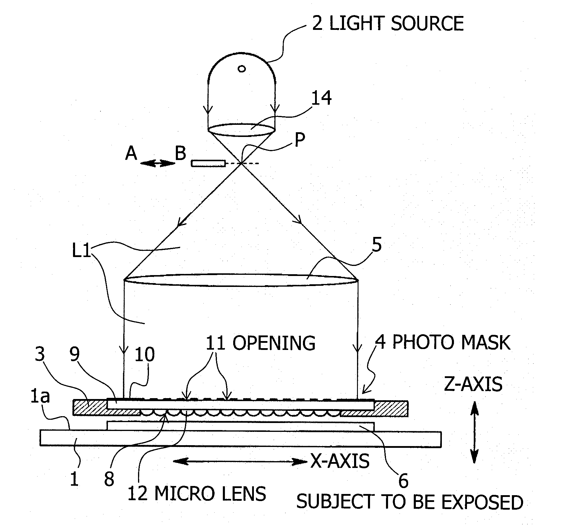
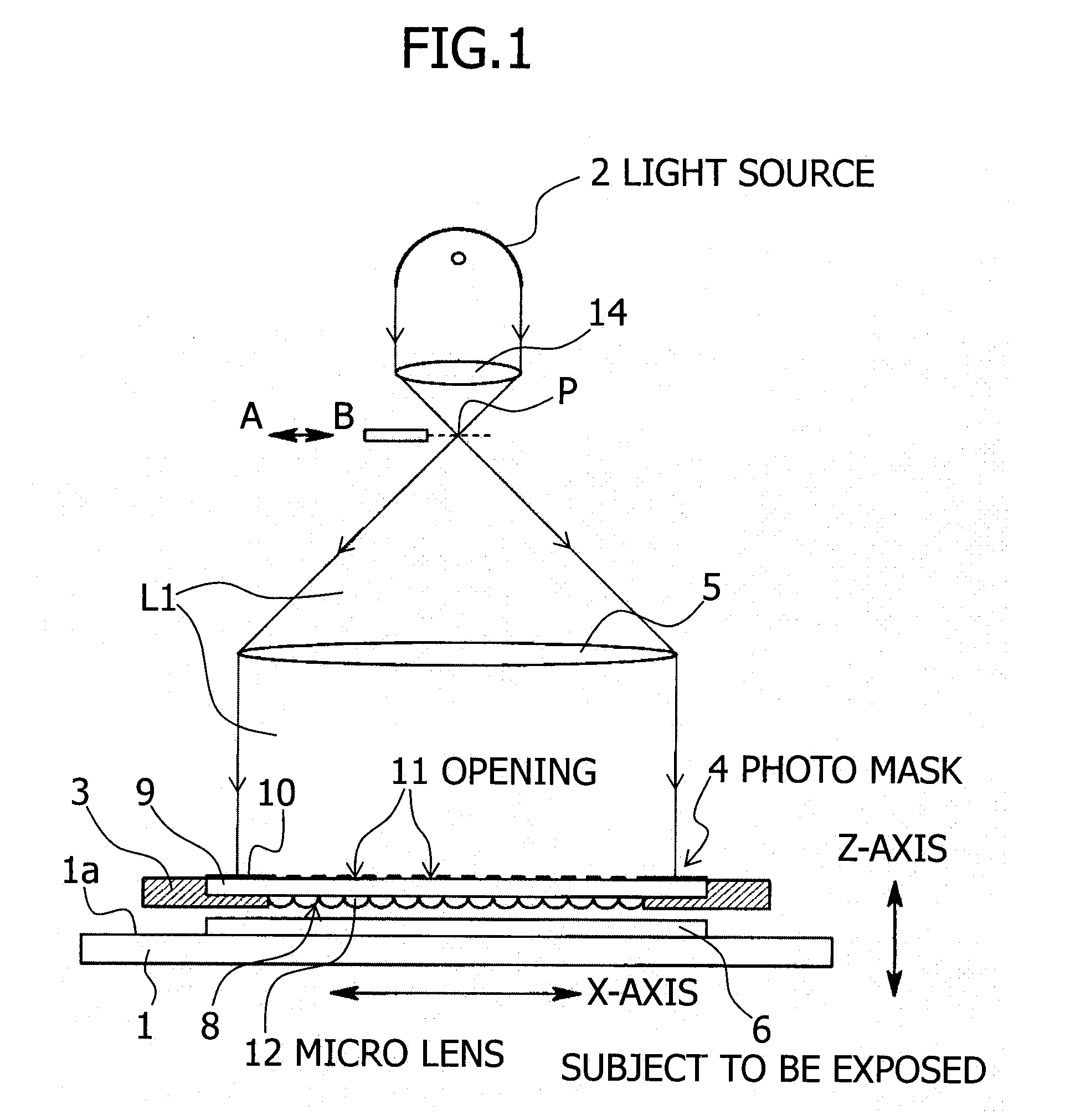
[0015]According to a first aspect of the exposure apparatus, the plurality of micro lenses are disposed on the side of the subject to be exposed in such a manner as to correspond to the openings formed in the photo mask, and the micro lens form the images of the openings on the subject to be exposed. In this manner, the resolution of the exposure pattern can be enhanced. Therefore, a fine pattern having a
line width of, for example, about 3 μm can be formed by proximity exposure. Hence, a pattern requiring a
high resolution such as a
transistor unit for a TFT substrate can be exposed and formed by using a proximity exposure apparatus which is inexpensive with a simple optical configuration, thereby reducing manufacturing cost of the TFT substrate.
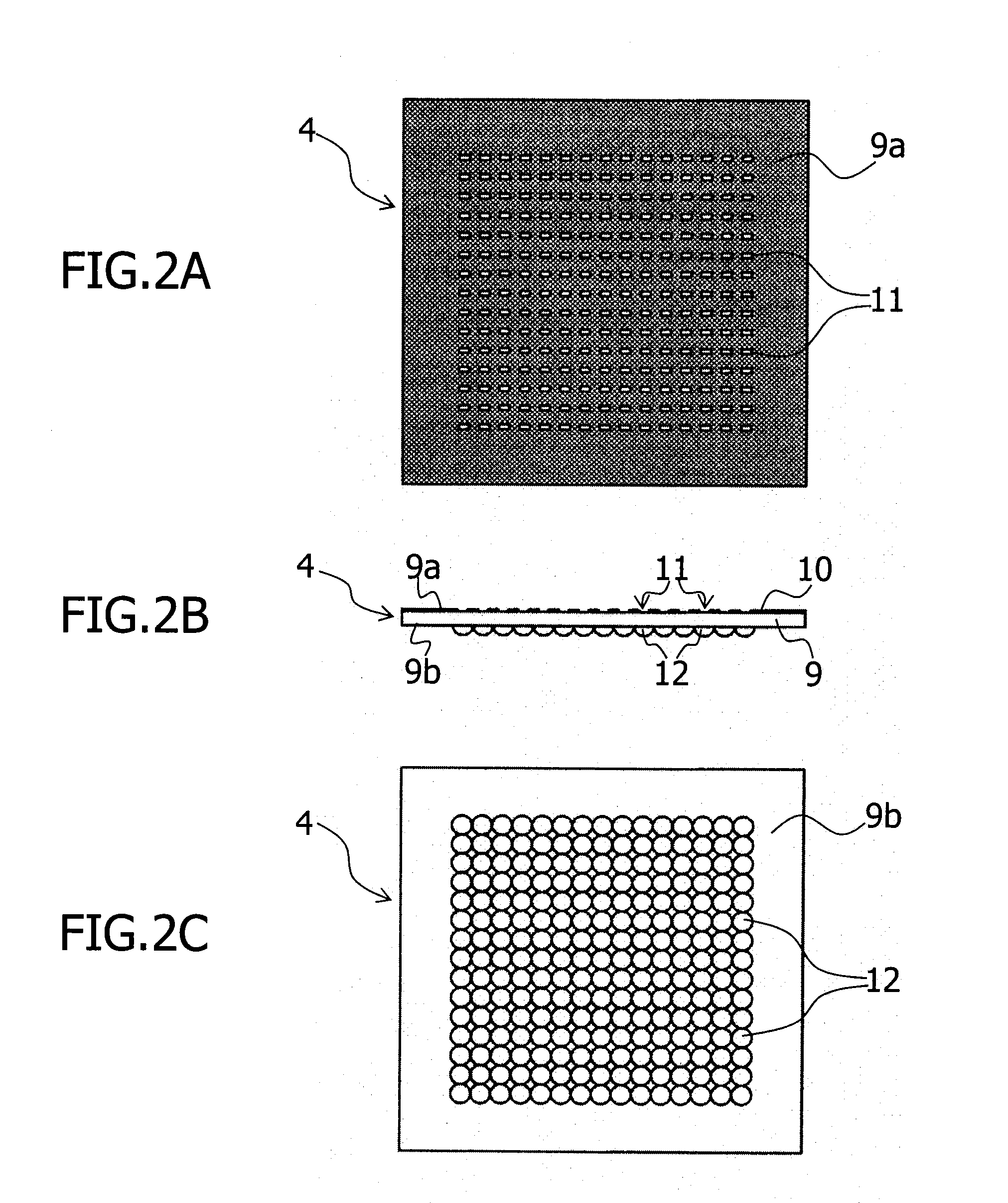
[0016]According to a second aspect of the invention, the micro lenses are formed on the surface of the transparent substrate, opposite to the surface having the openings formed therein, thereby dispensing with any positional alignment between the openings and the micro lenses. Thus, the photo mask can be readily treated.
[0017]According to a third aspect of the invention, the photo mask having the plurality of openings formed therein is formed independently of the micro lenses, and therefore, when the photo mask is deficient or a deficiency occurs later, only the photo mask may be replaced with a new one. Thus, it is possible to suppress an increase in cost of the photo mask.
[0018]According to a fourth aspect of the invention, the plurality of subjects to be exposed can be sequentially conveyed while being exposed to the
light beam, thereby increasing the number of subjects to be exposed per unit time. In the photo mask to be used in this case, at least the width of the subject to be exposed in the conveying direction may be smaller than that in an exposure region of the subjects to be exposed in the same direction, thereby reducing the size of the photo mask so as to reduce the manufacturing cost of the photo mask.
[0019]According to a fifth aspect of the photo mask, the plurality of openings are formed in the light shielding film disposed on one surface of the transparent substrate, and the plurality of micro lenses are disposed on the other surface in such a manner as to correspond to the openings, so that the micro lenses can form the images of the openings on the subject to be exposed which is disposed proximately and oppositely to the photo mask, thereby increasing the resolution of the exposure pattern. Therefore, a fine pattern having a
line width of, for example, about 3 μm can be formed by proximity exposure. Hence, a pattern requiring a
high resolution such as a
transistor unit for a TFT substrate can be exposed and formed by using a proximity exposure apparatus which is inexpensive with a simple optical configuration, thereby reducing a manufacturing cost of the TFT substrate.

