

A/d conversion device
- Summary
- Abstract
- Description
- Claims
- Application Information
AI Technical Summary
Benefits of technology
Problems solved by technology
Method used
Image

Examples
first embodiment
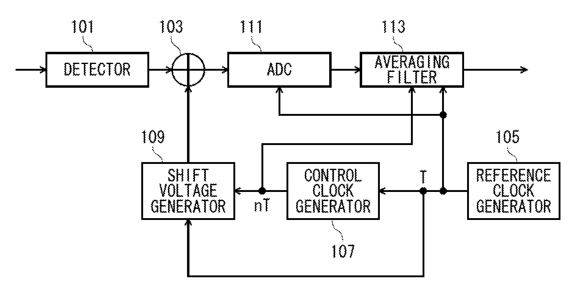
[0063]FIG. 1 is a block diagram showing an A / D conversion device of a first embodiment. As shown in FIG. 1, the A / D conversion device of the first embodiment includes a detector 101, an adder 103, a reference clock generator 105, a control clock generator 107, a shift voltage generator 109, an A / D converter (ADC: analog-to-digital converter) 111 and an averaging filter 113.
[0064]The detector 101 down-converts (performs frequency conversion of) a high frequency modulated signal received by an unillustrated antenna to a baseband. The adder 103 adds a shift voltage generated by the shift voltage generator 109 to a detected signal output by the detector 101, thereby offsetting a voltage level of a detected signal.
[0065]The reference clock generator 105 generates an operation clock signal for the ADC 111 and the averaging filter 113. An operation clock is called a “reference clock” having a cycle T in the following descriptions. In addition to the ADC 111 and the averaging filter 113, th...
second embodiment
[0100]FIG. 9 is a block diagram showing an A / D conversion device of a second embodiment.
[0101]In the A / D conversion device of the first embodiment, the adder 103 must be high precision in order to add a shift voltage to a detected signal.
[0102]In contrast, the A / D conversion device of the second embodiment has a reference voltage generator 201 and an adder 203, and a shift voltage similar to that described in connection with the first embodiment is added to a reference voltage used in each of the comparators of the ADC 111.
[0103]The A / D conversion device is similar to that described in connection with the first embodiment except the reference voltage generator 201 and the adder 203 shown in FIG. 9. In FIG. 9, parts that are identical with or equivalent to those of the A / D conversion device of the first embodiment shown in FIG. 1 are assigned the same or corresponding reference numerals, and their repeated explanations are simplified or omitted.
[0104]The voltages (the shift voltage a...
third embodiment
[0107]FIG. 10 is a block diagram showing an A / D conversion device of a third embodiment.
[0108]In the A / D conversion device of the third embodiment, a signal output from an operating condition changing section 303 is input to a detector 301. A gain of the detector 301 is set by means of an externally-input control voltage VH and a negative offset voltage value is set by means of an externally-input control voltage VL in such a way that a DC value of a signal which is output from the detector 301 and input to the ADC 111 becomes identical with or substantially equal to a DC value of the output from the adder 103 of the first embodiment.
[0109]The A / D conversion device of the third embodiment differs from the A / D conversion device of the first embodiment in that an offset of the detected signal is controlled by means of a voltage from the operating condition changing section 303 without use of the adder 103.
[0110]Constituent elements shown in FIG. 10 are analogous to their counterparts ...
PUM
 Abstract
Description
Claims
Application Information