

Mounting devices for optical devices, and related sub-assemblies, apparatuses, and methods
a technology of mounting devices and optical devices, applied in the direction of optical elements, circuit optical details, instruments, etc., can solve the problems of unfavorable signal integrity preservation, power transfer loss, and higher signal-to-noise ratios, so as to improve the grounding of optical devices and preserve signal integrity. , the effect of improving the shielding of radio frequency
- Summary
- Abstract
- Description
- Claims
- Application Information
AI Technical Summary
Benefits of technology
Problems solved by technology
Method used
Image

Examples
Embodiment Construction
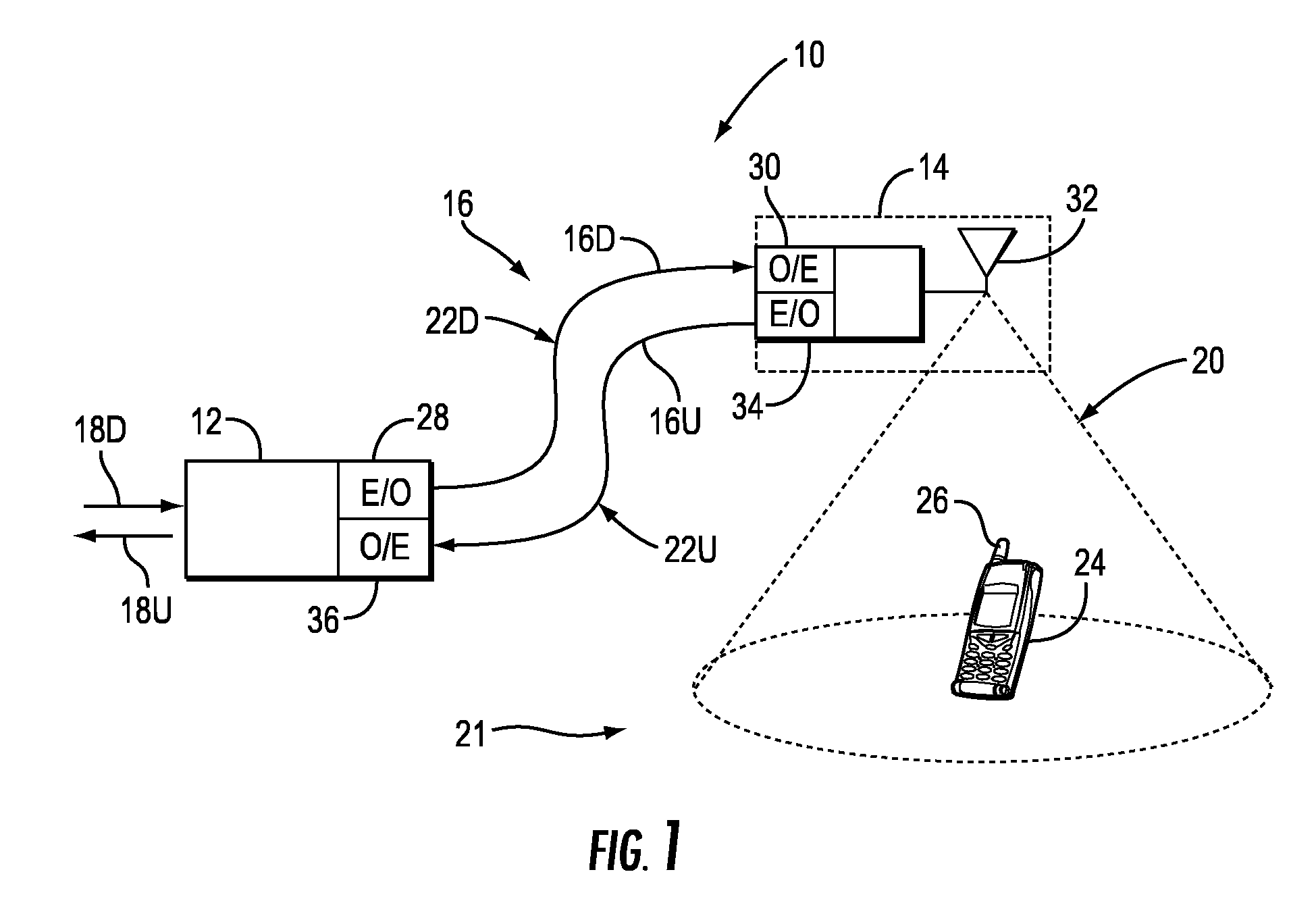
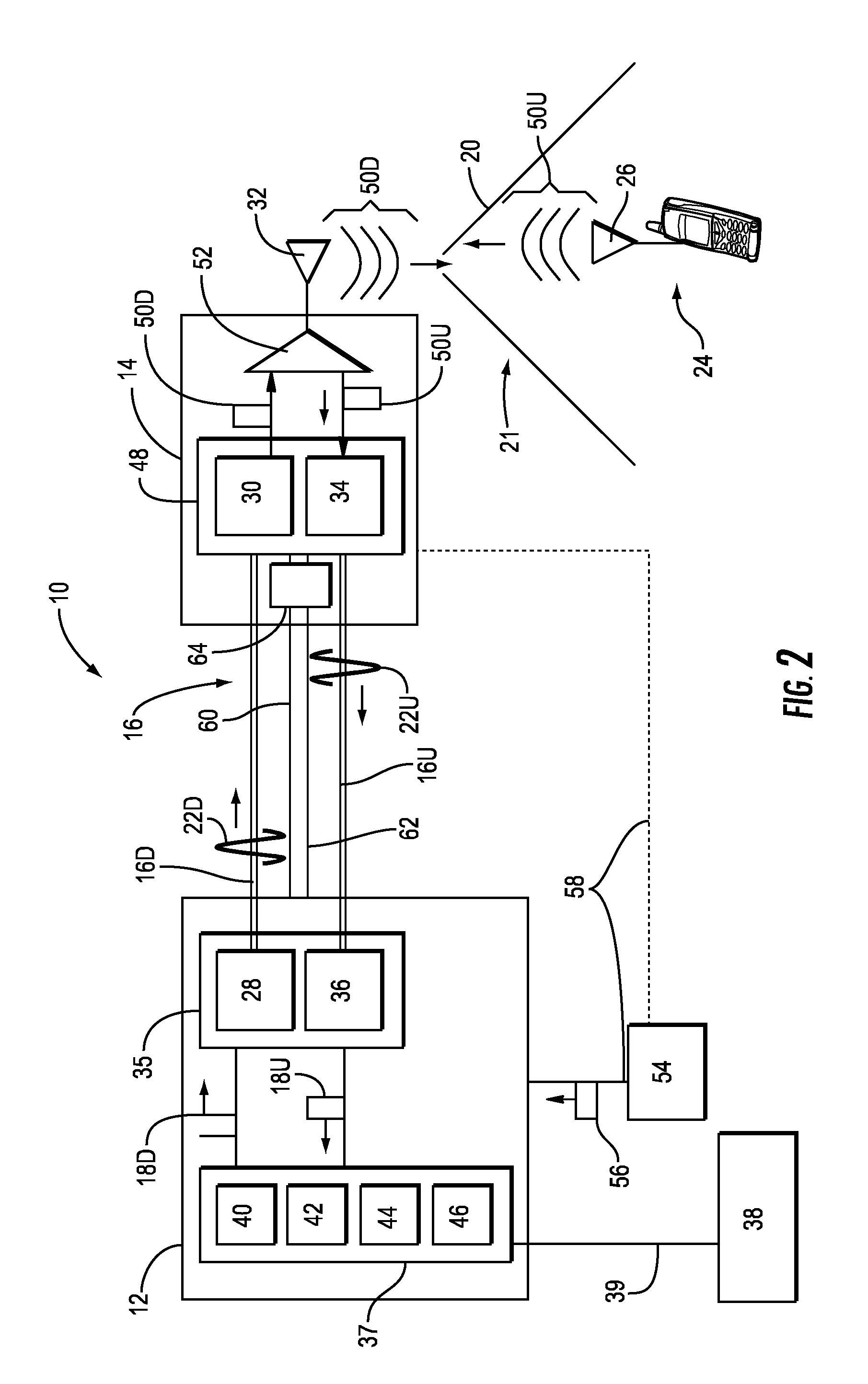
[0009]Embodiments disclosed in the detailed description include mounting devices for optical devices, and related sub-assemblies, apparatuses, and methods. The mounting devices may be employed to secure optical devices that are configured to convert optical signals to electrical signals, or electrical signals to optical signals. The mounting devices may be configured to secure optical devices to an electronics board, such as a printed circuit board (PCB) as an example. To preserve signal integrity, the mounting devices may also be configured to align the optical devices with electrical lead connections on the electronics board. The mounting devices may also be configured to improve grounding of the optical devices to provide and improve radio frequency (RF) shielding to avoid degradation of signal-to-noise (S / N) ratios from RF interference from electronic devices on the electronics board and other nearby electronic devices.
[0010]In this regard in one embodiment, a mounting device fo...
PUM
| Property | Measurement | Unit |
|---|---|---|
| radius | aaaaa | aaaaa |
| frequency | aaaaa | aaaaa |
| frequencies | aaaaa | aaaaa |
Abstract
Description
Claims
Application Information