Low power pulse signaling

a low-power pulse and signaling technology, applied in pulse manipulation, pulse technique, power consumption reduction, etc., can solve problems such as drawing considerable dc power

Inactive Publication Date: 2007-03-06
FULKERSON DAVID E
View PDF5 Cites 0 Cited by
  • Summary
  • Abstract
  • Description
  • Claims
  • Application Information

AI Technical Summary

Benefits of technology

[0008]The present invention is a system for communicating between integrated circuits. The system includes a driver having an input and an output. In response to a logic transition from a first logic state to a second logic state at the driver input, the driver output transitions from a low-power condition, to a transmitting condition, to the low-power condition. The system also includes a receiver having an input and an output. The receiver detects the logic state of the transmitting condition at the driver output and latches it to the receiver output after the driver output returns to the low-power condition. The system also includes a transmission line, which connects the driver output to the receiver input. The transition from the low-power condition to the transmitting condition and back to the low-power condition is done in a manner that maintains signal integrity at high speed and does not cause undesirable reflections or ringing on the transmission line.

Problems solved by technology

However, with LVDS the differential output constantly remains in a logic state, thus drawing considerable DC power.

Method used


Image

  • Low power pulse signaling
  • Low power pulse signaling
  • Low power pulse signaling

Examples


first embodiment

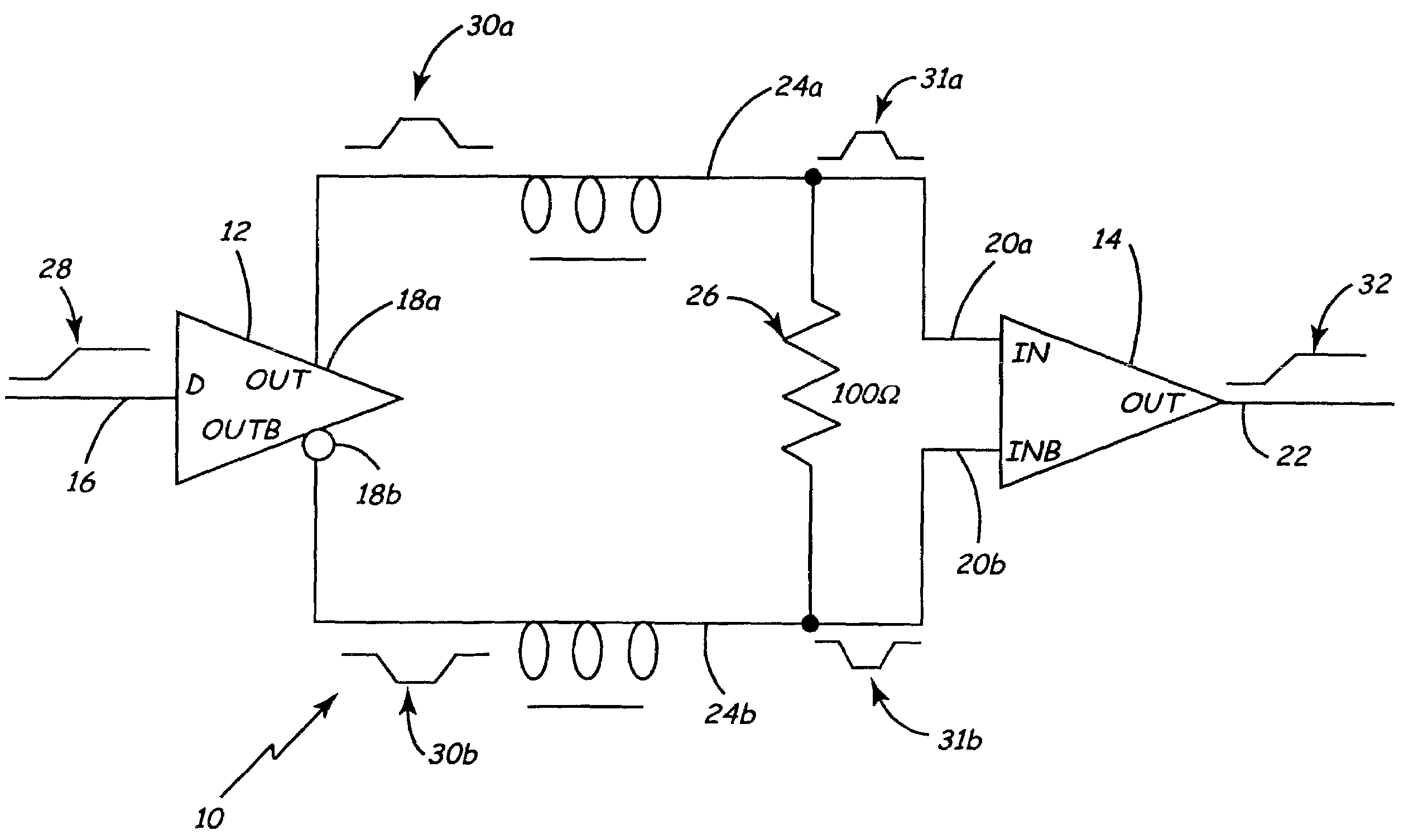
[0018]FIG. 1 is a schematic of low-power pulse signaling (LPPS) system 10 for communicating between on-chip or off-chip integrated circuits, according to the present invention. System 10 includes driver 12 and receiver 14. Driver 12 includes driver input 16, driver output 18a, and inverted driver output 18b. Receiver 14 includes receiver input 20a, inverted receiver input 20b, and receiver output 22. Driver output 18a is connected to receiver input 20a via transmission line 24a. Inverted driver output 18b is connected to inverted receiver input 20b via transmission line 24b. Transmission line 24a and transmission line 24b are terminated by resistor 26 at receiver 14.

[0019]In operation of low-power pulse signaling system 10, driver 12 receives signal 28 at driver input 16. Signal 28 is provided by other integrated circuitry (not shown), such as clocking circuitry or data circuitry. When signal 28 changes its logic state (that is, changes from a logic “0” to a logic “1” or from a logi...

second embodiment

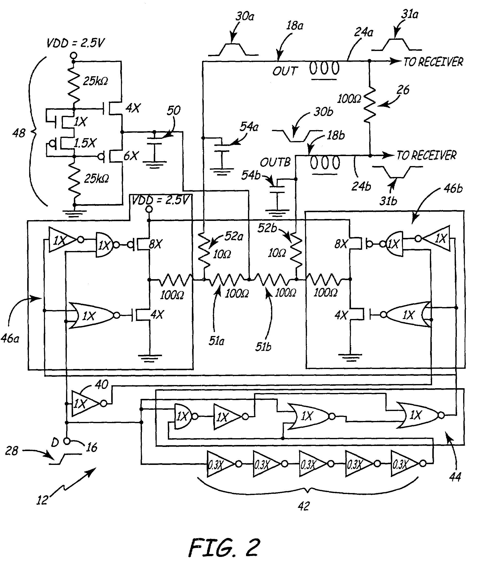
[0027]FIG. 3 is a detailed schematic of low-power pulse signaling driver circuit 12 of FIG. 1 with terminated transmission line 24 and output pulse height detector circuit 60. Driver circuit 12 includes driver input 16, signal inverter 62, delay inverters 64, pulse logic 66, set-reset latch 67, transistor driver logic 68a, inverted transistor driver logic 68b, low-power common mode voltage circuit 70, capacitor 72, driver terminating resistors 73a and 73b, electrostatic discharge (ESD) resistors 74a and 74b, and ESD capacitors 76a and 76b.

[0028]In operation of driver circuit 12, driver input 16 receives signal 28. As described above, signal 28 is provided by other integrated circuitry (not shown), such as clocking circuitry or data circuitry. While signal 28 maintains a steady logic state, a low-power non-logic state is maintained at outputs 18a and 18b by transistor driver logic 68a and inverted transistor driver logic 68b, respectively. When signal 28 changes its logic state, a s...


PUM


Abstract

A system for communicating between integrated circuits is disclosed. The system includes a driver having an input and an output. In response to a logic transition from a first logic state to a second logic state at the driver input, the driver output transitions from a low-power condition, to a transmitting condition, to the low-power condition. The system also includes a receiver having an input and an output. The receiver detects the logic state of the transmitting condition at the driver output and latches it to the receiver output after the driver output returns to the low-power condition. The system also includes a transmission line, which connects the driver output to the receiver input.

Description

CROSS-REFERENCE TO RELATED APPLICATION(S)[0001]This application claims priority from Provisional Application No. 60 / 311,049 filed Aug. 8, 2001, for “Low-Power Pulse Signaling” by D. Fulkerson.BACKGROUND OF THE INVENTION[0002]The present invention relates to high-speed integrated circuit output / input signaling, and more particularly to a low-power pulse signaling (LPPS) circuit.[0003]A variety of electronic systems rely on improvements in high-speed signaling to increase performance. Networks can operate at higher data rates when signals are propagated more quickly between stations and within network switches. Telephone systems can handle more calls when faster transmission occurs. At high data rates, the media through which signals are transmitted on a printed circuit board or within integrated circuit packages has characteristics similar to the transmission media in the aforementioned systems. Thus, constant improvements to signaling at this level are also necessary.[0004]An exampl...

Claims


Application Information

Patent Timeline
Patent Type & Authority Patents(United States)
IPC IPC(8): H04B1/38
CPCH03K5/1515H03K19/0013H03K19/0016H04L25/0292H04L25/0286H03K19/01707H04L25/0272
Inventor FULKERSON, DAVID E.
Owner FULKERSON DAVID E
Why Eureka
Try Eureka