Large-Scale X-Ray Detectors

a detector and large-scale technology, applied in the direction of optical radiation measurement, radiation control devices, instruments, etc., can solve the problems of difficult to form the hole in the asic corresponding to the position of an upper electrode, the tissue existing within the seam may not be detected, and the equipment that is not generally used for a silicon process is employed. achieve the effect of accurately reproducing and easy embodied

Inactive Publication Date: 2012-09-06
SAMSUNG ELECTRONICS CO LTD
View PDF3 Cites 34 Cited by
  • Summary
  • Abstract
  • Description
  • Claims
  • Application Information

AI Technical Summary

Benefits of technology

[0012]The X-ray detector may further include resin between the printed circuit board and the chips. The photoconductor may be formed of at least one material selected from the group consisting of amorphous selenium (a-Se), HgI2, PbI2, CdTe, CdZnTe, and PbO. According to example embodiments including a large-scale X-ray detector, because wire bonding is performed using a gap between the chips without penetrating the chips for a connection from the pin pads of the chip to a lower portion of the chip, a large-scale X-ray detector may be easily embodied. Because electric charges generated on the photoconductor in a seam area between the chip areas are transmitted to the chip via the pixel electrodes thereunder, an image of a seamless photography area may be accurately reproduced.

Problems solved by technology

Specifically, during the tiling of ASICs, a seam having a size of at least 100 μm may be generated, thus tissues existing within the seam may not be detected.
To perform the process, expensive equipment that is not generally used for a silicon process is employed.
The process is performed at high temperature that may damage the ASIC.
Also, it is difficult to form the hole in the ASIC corresponding to the position of an upper electrode.

Method used


Image

  • Large-Scale X-Ray Detectors
  • Large-Scale X-Ray Detectors
  • Large-Scale X-Ray Detectors

Examples


Embodiment Construction

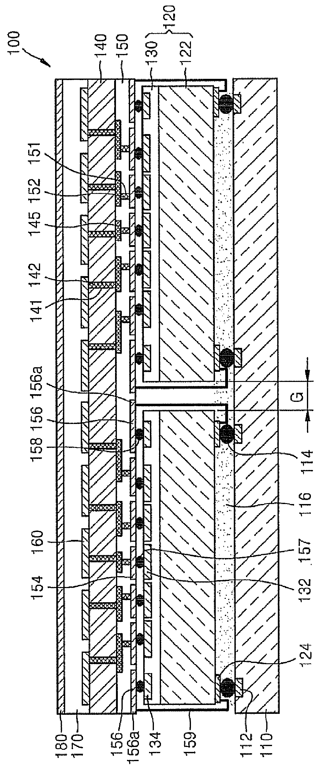
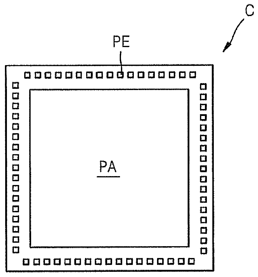
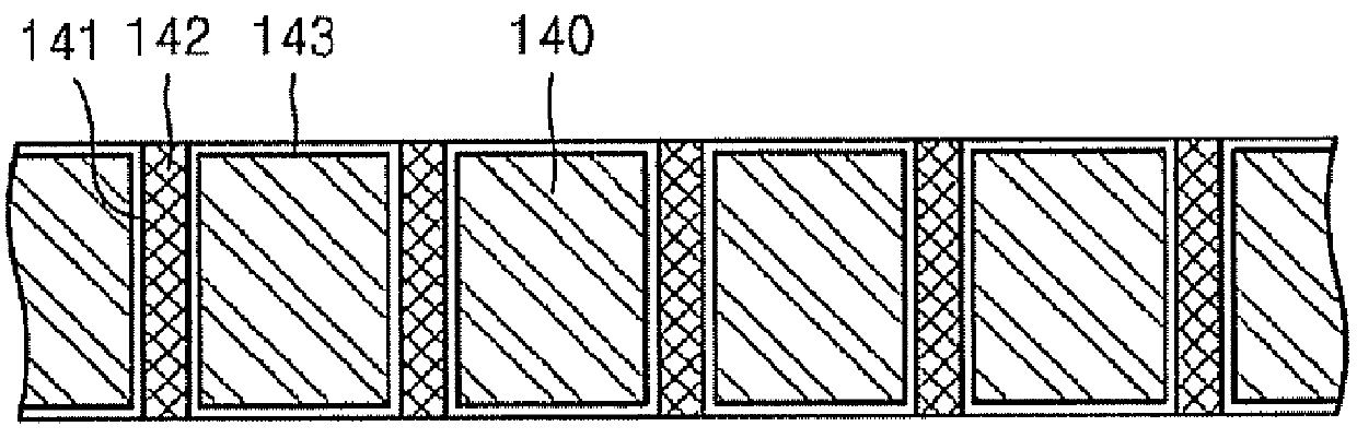
[0020]Example embodiments will now be described more fully with reference to the accompanying drawings, in which example embodiments are shown. Example embodiments may, however, be embodied in many different forms and should not be construed as being limited to the embodiments set forth herein; rather, these embodiments are provided so that this disclosure will be thorough and complete, and will fully convey the concept of example embodiments to those of ordinary skill in the art. In the drawings, the thicknesses of layers and regions are exaggerated for clarity. Like reference numerals in the drawings denote like elements, and thus their description will be omitted.

[0021]It will be understood that when an element is referred to as being “connected” or “coupled” to another element, it can be directly connected or coupled to the other element or intervening elements may be present. In contrast, when an element is referred to as being “directly connected” or “directly coupled” to anot...


PUM


Abstract

An X-ray detector including a plurality of chips on a printed circuit board, each of the plurality of chips including a plurality of pixel pads on a center portion of the printed circuit board and a plurality of pin pads surrounding the plurality of pixel pads, a plurality of pixel electrodes on and corresponding to the plurality of chips, a redistribution layer electrically connecting the plurality of pixel electrodes and the plurality of pixel pads, a plurality of first electrode pads on a surface opposite to a surface of the plurality of chips including the plurality of pin pads, a wire electrically connecting the plurality of first electrode pads and the plurality of pin pads, a photoconductor on the plurality of pixel electrodes, and a common electrode on the photoconductor.

Description

CROSS-REFERENCE TO RELATED APPLICATIONS[0001]This application claims priority under 35 U.S.C. §119 to Korean Patent Application No. 10-2011-0019646, filed on Mar. 4, 2011, in the Korean Intellectual Property Office (KIPO), the entire contents of which is incorporated herein by reference.BACKGROUND[0002]1. Field[0003]Example embodiments relate to large-scale X-ray detectors that may realize seamless images.[0004]2. Description of the Related Art[0005]A digital X-ray detector outputs an X-ray image photograph or an X-ray fluoroscopic image using an X-ray in form of digital signals. An X-ray detector may be a direct type and / or an indirect type. According to the direct type, a photoconductor directly converts an X-ray to electric charges. In the indirect type, a scintillator converts an X-ray to a visible ray and a photoelectric conversion device such as a photodiode converts a converted visible ray to electric charges.[0006]A direct type X-ray detector includes a plurality of pixel el...

Claims


Application Information

Patent Timeline
Patent Type & Authority Applications(United States)
IPC IPC(8): H01L27/146G01T1/24G01T1/16
CPCH01L27/14676H01L27/14618H01L2924/0002H01L2924/00G01N23/04G01T1/24H01L31/085
Inventor KIM, SANG-WOOKKIM, CHANG-JUNGPARK, JAE-CHULKIM, SUN-IL
Owner SAMSUNG ELECTRONICS CO LTD
Why Eureka
Try Eureka