Two-stage post driver circuit

a post driver circuit and two-stage technology, applied in the field of post driver circuits, can solve the problems of increased failure to operate normally in the two-stage post driver circuit, etc., and achieve the effect of minimizing the adverse effect and minimizing the possibility of damage to the transistor

Active Publication Date: 2012-09-06
GLOBAL UNICHIP CORPORATION +1
View PDF1 Cites 1 Cited by
  • Summary
  • Abstract
  • Description
  • Claims
  • Application Information

AI Technical Summary

Benefits of technology

[0015]Therefore, the present invention provides two-stage post driver circuit to minimize the adverse affect arising from the difference between the drain voltage and the source voltage of the transistor at the moment when the pull-down unit or the pull-up unit is turned on. Consequently, the possibility of damaging the transistor will be minimized.

Problems solved by technology

Under this circumstance, the first P-type transistor P1 is possibly burned out, and thus the two-stage post driver circuit fails to be normally operated.
Consequently, the possibility of damaging the transistor is increased.

Method used


Image

  • Two-stage post driver circuit
  • Two-stage post driver circuit
  • Two-stage post driver circuit

Examples


Embodiment Construction

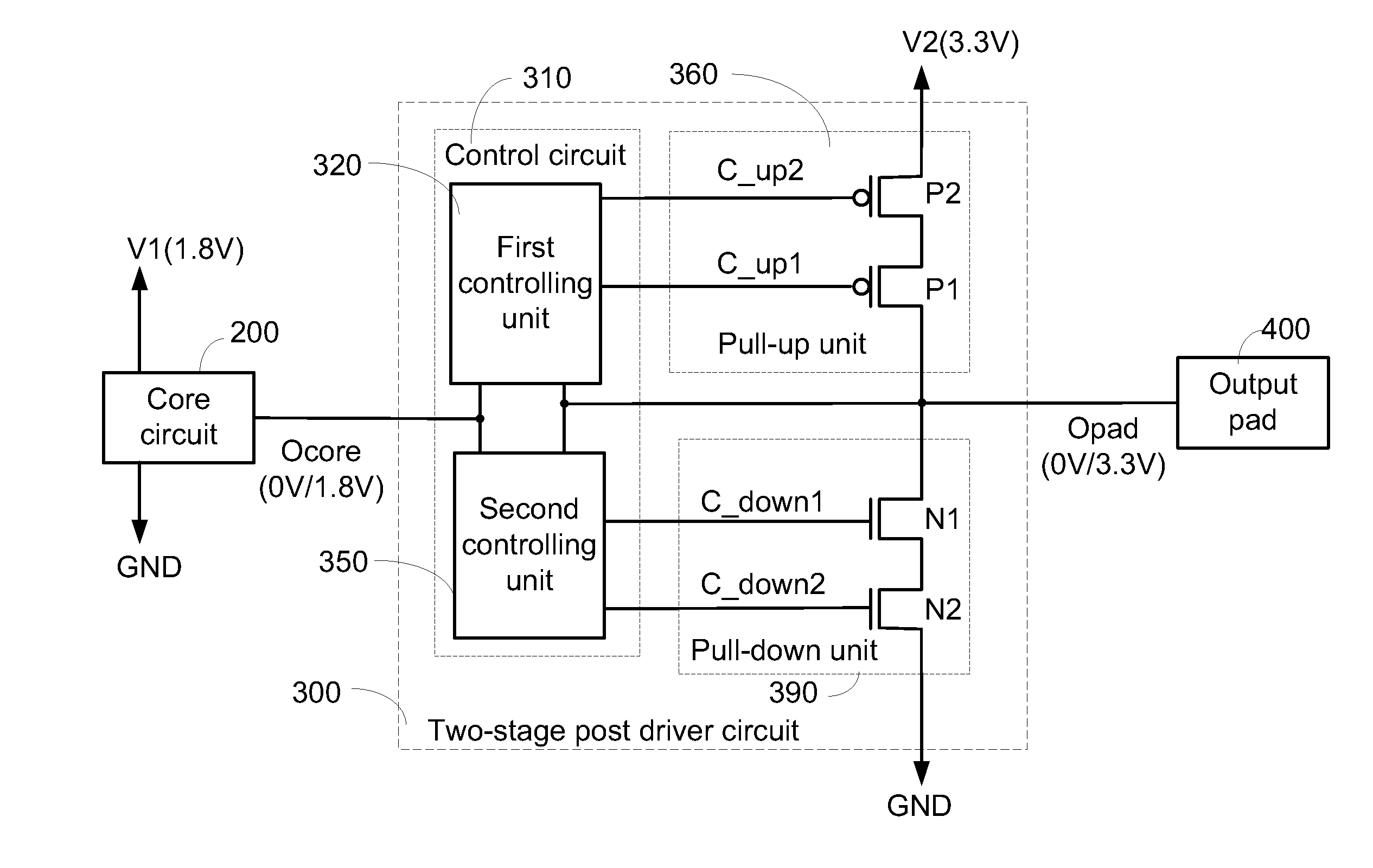
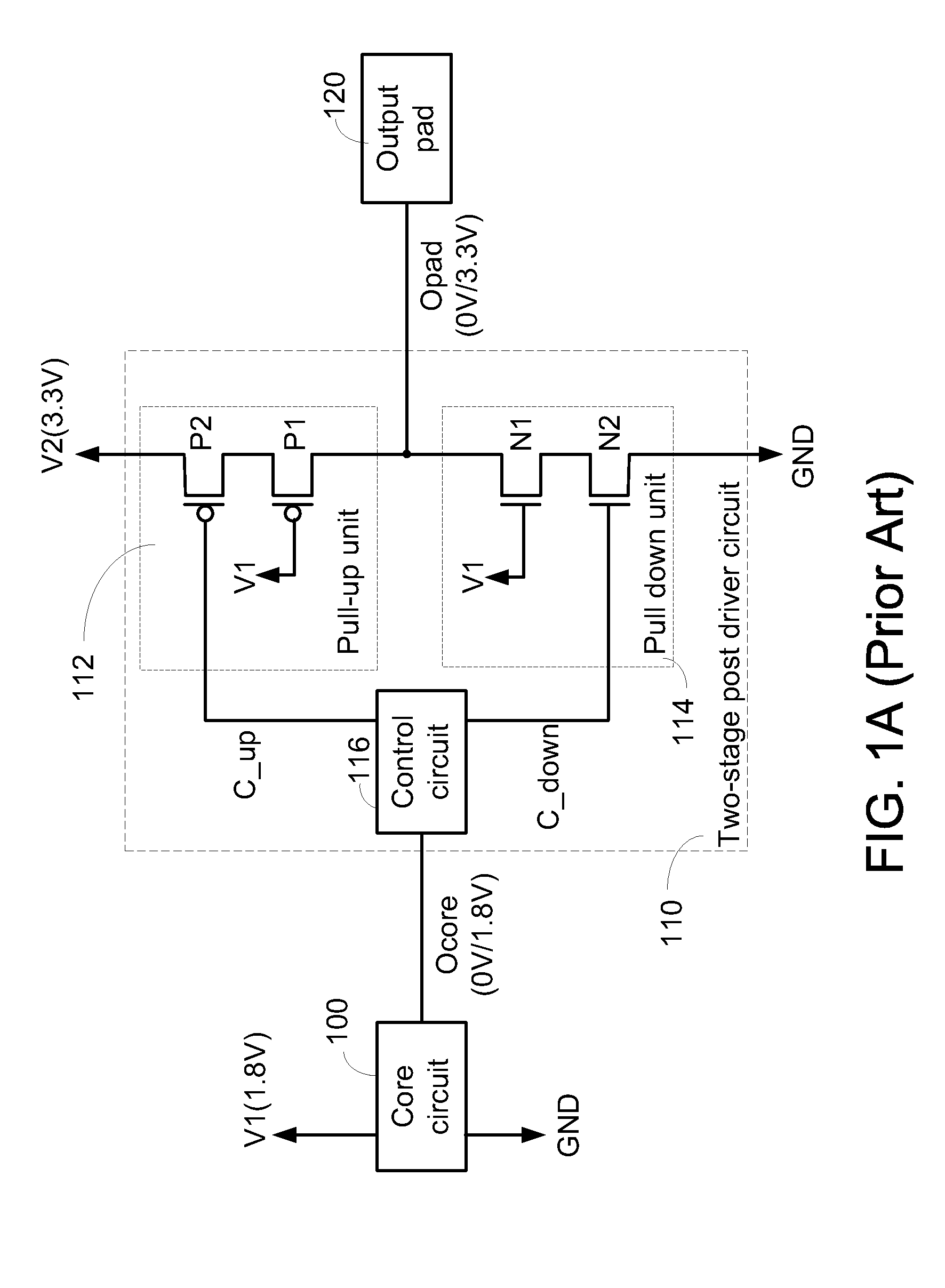
[0028]In the conventional two-stage post driver circuit, the gate terminal of the first N-type transistor and the gate terminal of the first P-type transistor are both connected to a constant voltage (V1). When the pull-up unit or the pull-down unit is turned on, the gate voltage fails to provide sufficient pull-up strength or pull-down strength. Since the voltage difference between the drain terminal and the source terminal is too large, the first P-type transistor P1 or the first N-type transistor N1 is easily damaged. For obviating the drawbacks encountered from the prior art, the present invention provides an improved two-stage post driver circuit.

[0029]FIG. 2 is a schematic circuit diagram illustrating a two-stage post driver circuit according to an embodiment of the present invention. The two-stage post driver circuit 300 is connected between a core circuit 200 and an output pad 400. The core circuit 200 is connected between a first source voltage V1 and a ground terminal GND....


PUM


Abstract

A two-stage post driver circuit includes a controlling circuit, a pull-up unit and a pull-down unit. A first N-type transistor of the pull-down unit and a first P-type transistor of the pull-up unit are both connected to an output pad. The controlling circuit is used for controlling the first N-type transistor and the first P-type transistor. Consequently, when the pull-up unit or the pull-down unit is turned on, the voltage difference between the drain terminal and the source terminal of the first N-type transistor or the first P-type transistor is lower than a voltage stress.

Description

[0001]This application claims the benefit of Taiwan Patent Application No. 100106975, filed Mar. 2, 2011, the subject matter of which is incorporated herein by reference.FIELD OF THE INVENTION[0002]The present invention relates to a post driver circuit, and more particularly to a two-stage post driver circuit.BACKGROUND OF THE INVENTION[0003]During the process of packaging an integrated circuit, for making the IC chip to be connected with the package pins, the internal IC chip is usually equipped with a core circuit for providing main functions, and input / output pads are located between the core circuit and the external package pins. For designing the output pads and the input pads as the bridge between the core circuit and the external package pins, some additional factors should be taken into consideration because of the special properties thereof. Take an output pad for example. For providing sufficient driving capability, a post driver circuit is necessary for the output pad.[00...

Claims


Application Information

Patent Timeline
Patent Type & Authority Applications(United States)
IPC IPC(8): H03K5/00
CPCH03K19/00315H03K17/08104H03K19/00361
Inventor WANG, WEN-TAIHUANG, CHAO-YEN
Owner GLOBAL UNICHIP CORPORATION
Why Eureka
Try Eureka