
Touch panel and touch pad

a touch panel and touch pad technology, applied in the field of touch technology, can solve the problems of difficult adjustment of the capacitance type of the reciprocal capacitance, the capacitance type touch panel transmittance drop, and the size of the panel and the number, so as to increase the capacitance of the sensing channel toward ground, increase the touch area, and enhance the sensitivity of the touch pad.

Inactive Publication Date: 2012-09-06
RAYDIUM SEMICON
View PDF3 Cites 6 Cited by
  • Summary
  • Abstract
  • Description
  • Claims
  • Application Information

AI Technical Summary

Benefits of technology

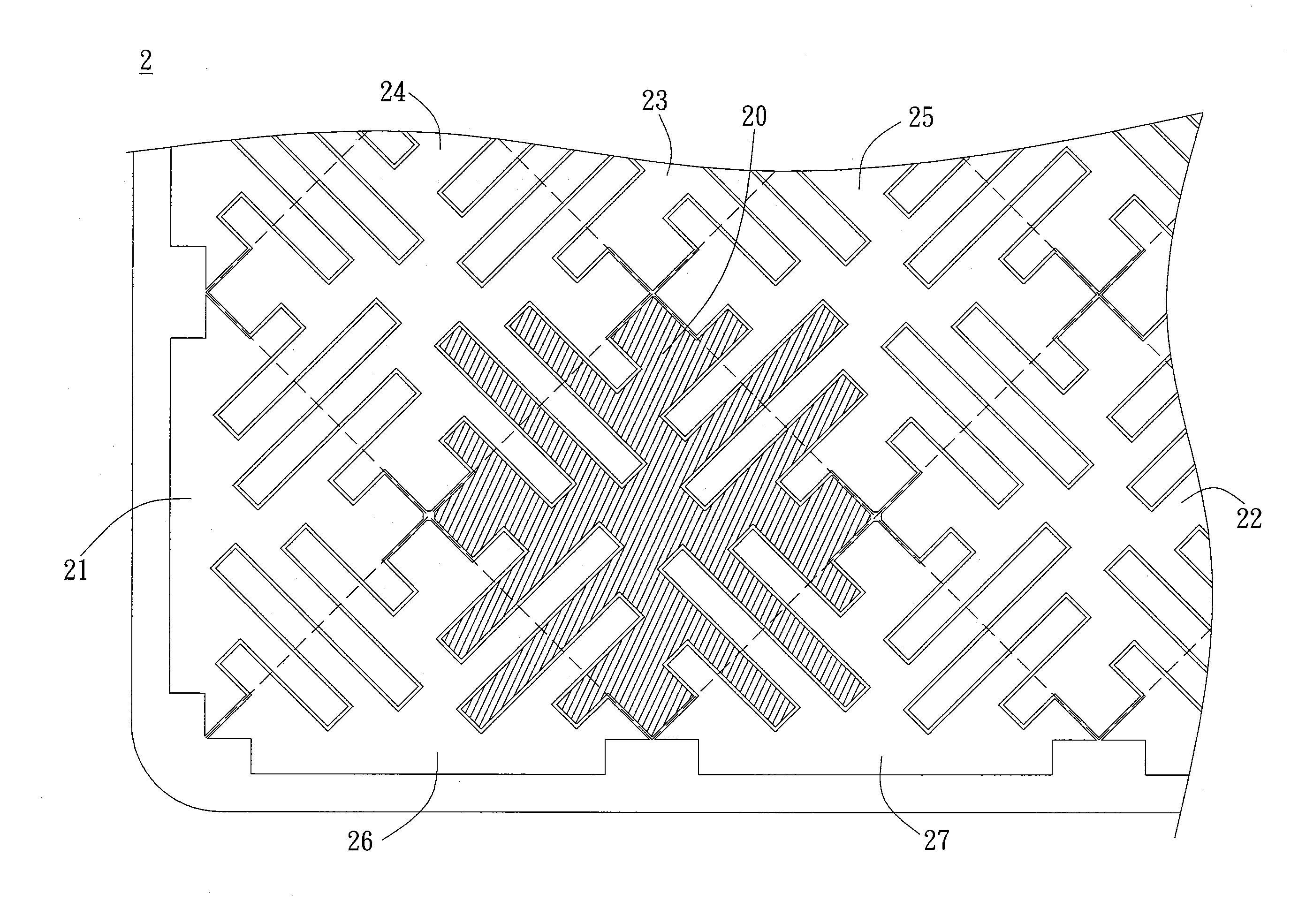
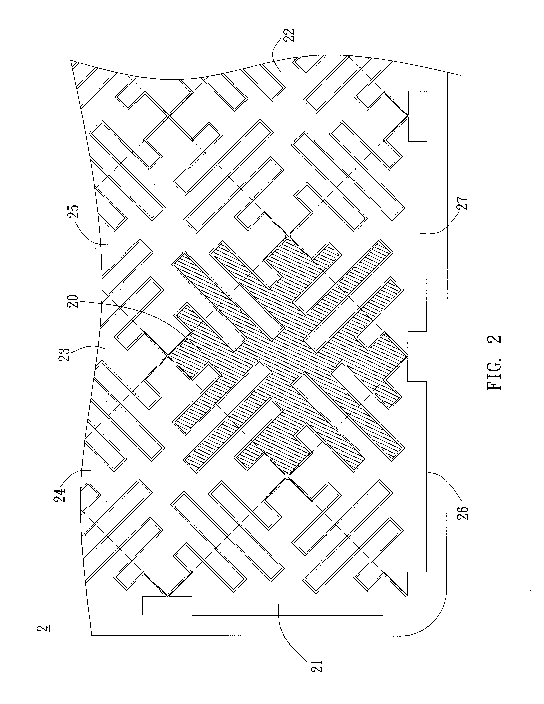
The invention provides a touch pad and touch panel with improved sensitivity and signal-noise ratio. The touch pad has symmetrical edges with a first region surrounded by a convex and a concave, and a second region surrounded by a concave and a convex. The touch panel includes a plurality of touch pads that can be embedded in each other to increase the touch area and mutual capacitance between the driving and sensing channels. The non-driving or non-sensing channels can be set to increase the capacitance of the sensing channel towards ground and enhance its resistance to noises. The invention maintains the advantage of the conventional diamond structure while increasing the competitiveness of the touch panel on the market.

Problems solved by technology

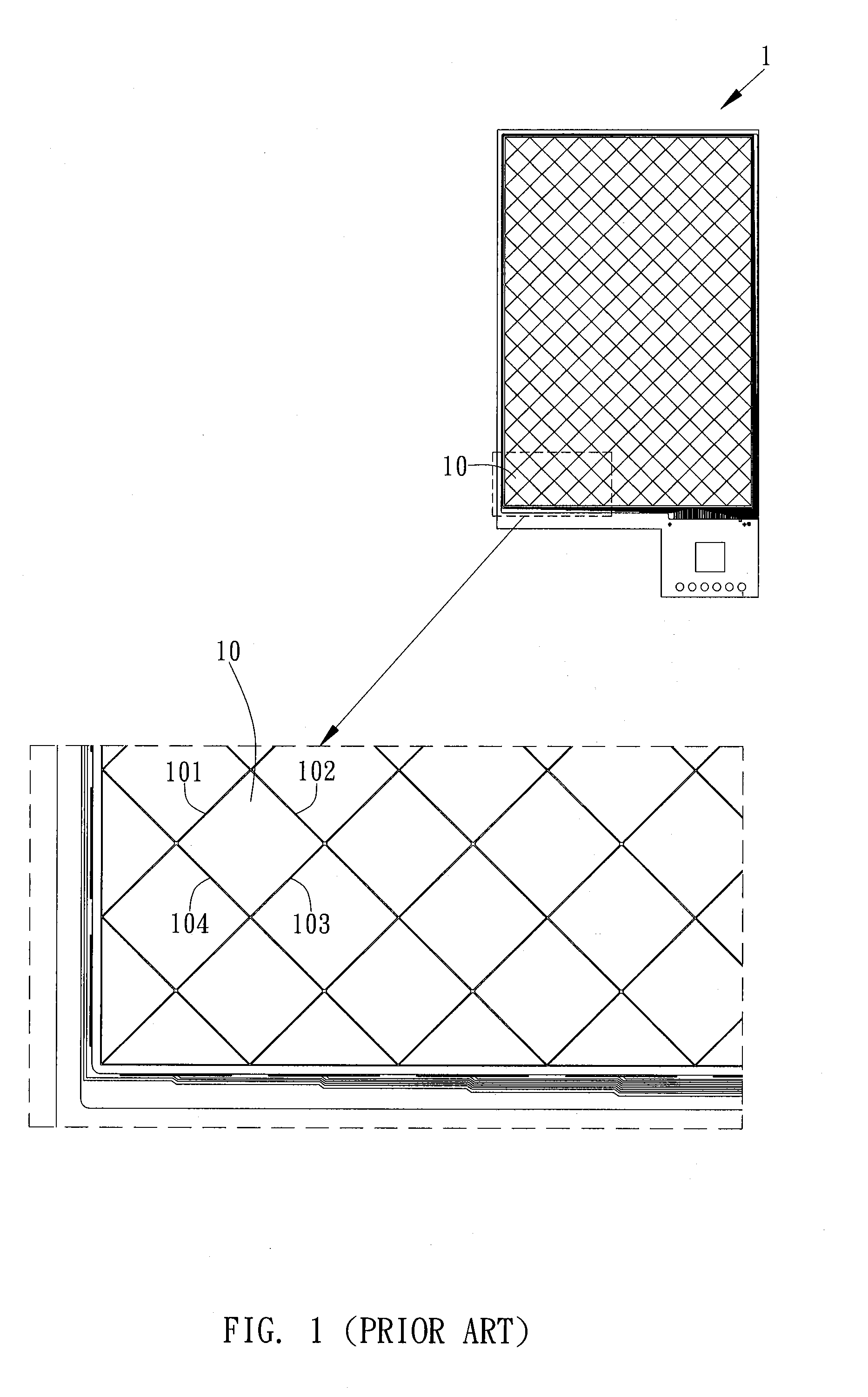
However, for the touch pad 10 having the diamond structure shown in FIG. 1, its mutual capacitance is hard to be adjusted since it is limited by the lengths of the four edges 101˜104 of the touch pad 10, that is to say, indirectly limited by the size of the panel and the number of the sensing pins.
Although the capacitance type touch panel can also use another touch pad having the strip structure to increase the sensitivity of the touch pad and improve the signal to noise ratio (SNR) by adjusting the size of the overlapping region between the driving channel and the sensing channel and the distance between two layers of ITO glass, in practical applications, this strip structure should use two layers of ITO glass not only leading to the transmittance of the capacitance type touch panel drop but also causing high production cost.

Method used


Image

  • Touch panel and touch pad
  • Touch panel and touch pad
  • Touch panel and touch pad

Examples


Embodiment Construction

[0023]The invention provides a touch panel and a touch pad thereof, it is to change the shape of the edges of the touch pads and maintain the original area of the touch pad, so that the touch pads of vertical direction and horizontal direction can be embedded each other to increase the touch area and the mutual capacitance between the driving channel and the sensing channel, and the sensitivity of the touch pad can be also enhanced.

[0024]An embodiment of the invention is a touch panel. In this embodiment, the touch panel is a capacitance type touch panel, and the touch panel includes a plurality of touch pads. Please refer to FIG. 2. FIG. 2 illustrates a schematic diagram of the touch panel including the plurality of touch pads in the invention.

[0025]As shown in FIG. 2, the touch panel 2 includes a plurality of touch pads 20˜27, and the plurality of touch pads 20˜27 is alternately aligned in a vertical direction and a horizontal direction to be used as driving channels and sensing c...


PUM


Abstract

A touch panel and a plurality of touch pads thereof are disclosed. Each touch pad includes a plurality of the same edges. Each edge includes two edge ends, an edge center, at least one convex, and at least one concave. A line between the two edge ends is defined as a reference line. The edge center is located at the center of the reference line. A first region is surrounded by the at least one convex and the reference line. A second region is surrounded by the at least one concave and the reference line. The at least one convex and the at least one concave are symmetrical to the edge center.

Description

BACKGROUND OF THE INVENTIONCross-Reference to Related Application[0001]This application claims priority based on Taiwanese Patent Application No. 100107304, filed on Mar. 4, 2011, the disclosure of which is incorporated herein by reference in its entirety.FIELD OF THE INVENTION[0002]The invention relates to the touch technology; in particular, to a touch pad capable of enhancing the sensitivity of the touch panel effectively and a touch panel including the touch pad.[0003]DESCRIPTION OF THE PRIOR ART[0004]In recent years, with the development of the touch technology, inputting by touch has become the main trend input way of the human machine interface. As a new generation of smart phones and other consumer electronics products come out, the touch screen has become more popular, the touch panel market for the future is also very optimistic about growth prospects. Especially, after the next generation Windows operating system can support the touch panel, the touch panel can be applied...

Claims


Application Information

Patent Timeline
Patent Type & Authority Applications(United States)
IPC IPC(8): G06F3/041
CPCG06F3/0418G06F2203/04111G06F3/044G06F3/0448G06F3/0446G06F3/0443
Inventor YANG, CHEN-WEILIN, WEN-TSUNGSHICH, HSIN-WEI
Owner RAYDIUM SEMICON
Learn More