Method of Fabricating Semiconductor Device

Active Publication Date: 2012-09-06
UNITED MICROELECTRONICS CORP
View PDF3 Cites 22 Cited by
  • Summary
  • Abstract
  • Description
  • Claims
  • Application Information

AI Technical Summary

Benefits of technology

[0009]The present invention provides a method of fabricating a semiconductor device to substantially form a high-voltage device and a low-voltage device. By using the

Problems solved by technology

With a trend toward scaling down the size of semiconductor devices, the conventional poly-silicon gate has faced problems such as inferior performance due to boron penetration and unavoidable depletion effect which increases equivalent thickness of the gate dielectric layer, reduces gate capacitance, and worsens a driving force of the devices.
However, because of t

Method used


Image

  • Method of Fabricating Semiconductor Device
  • Method of Fabricating Semiconductor Device
  • Method of Fabricating Semiconductor Device

Examples


Embodiment Construction

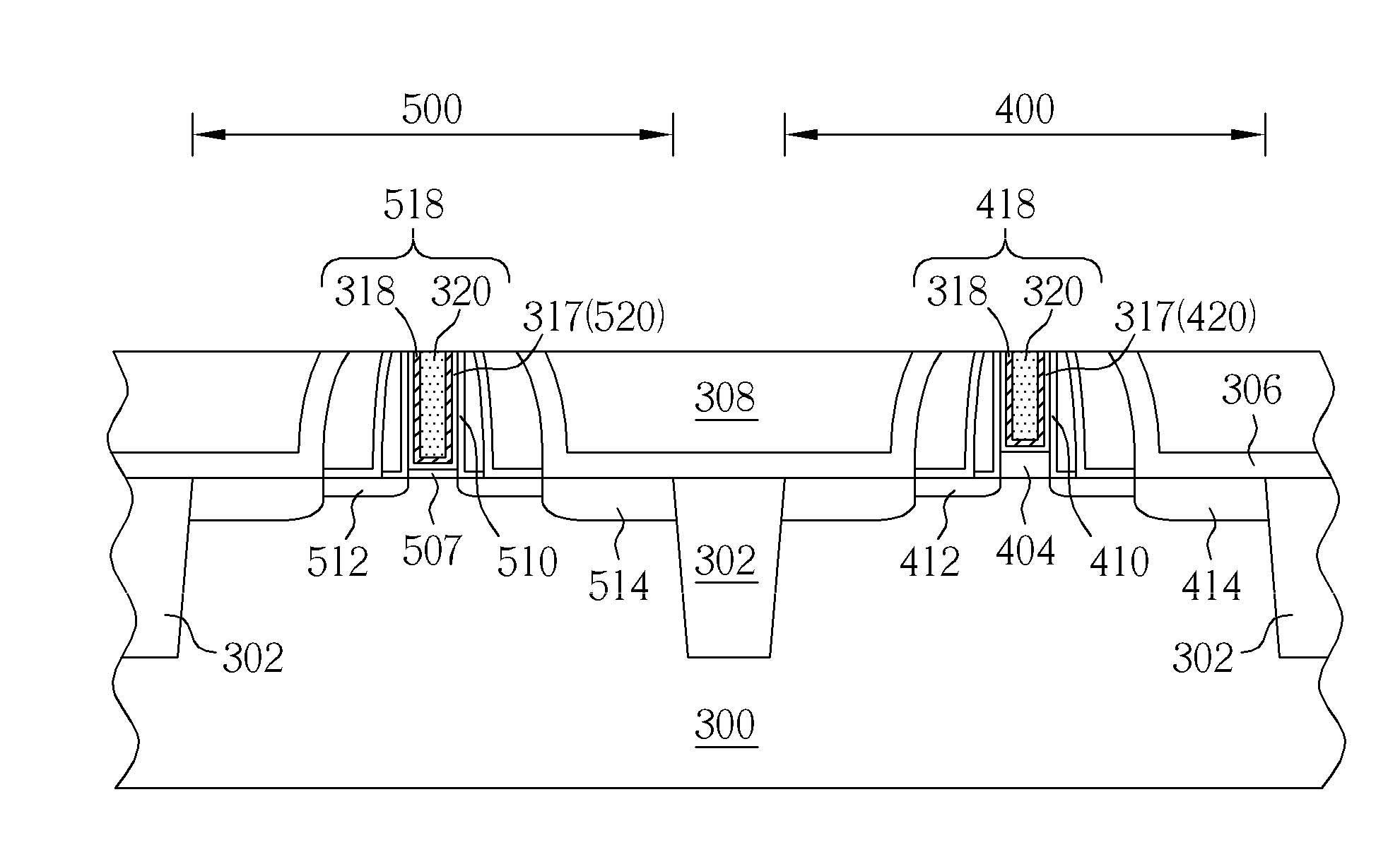
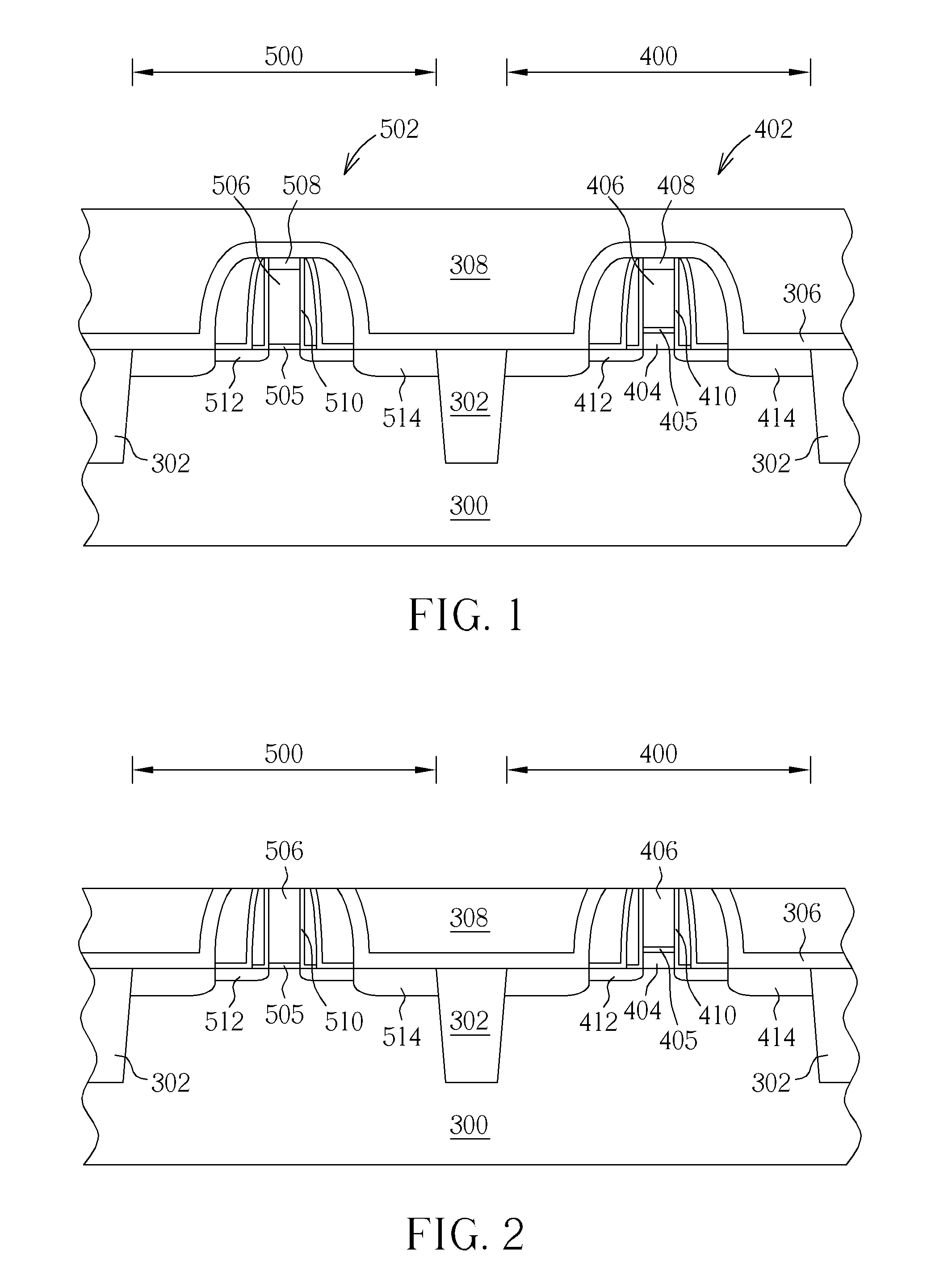
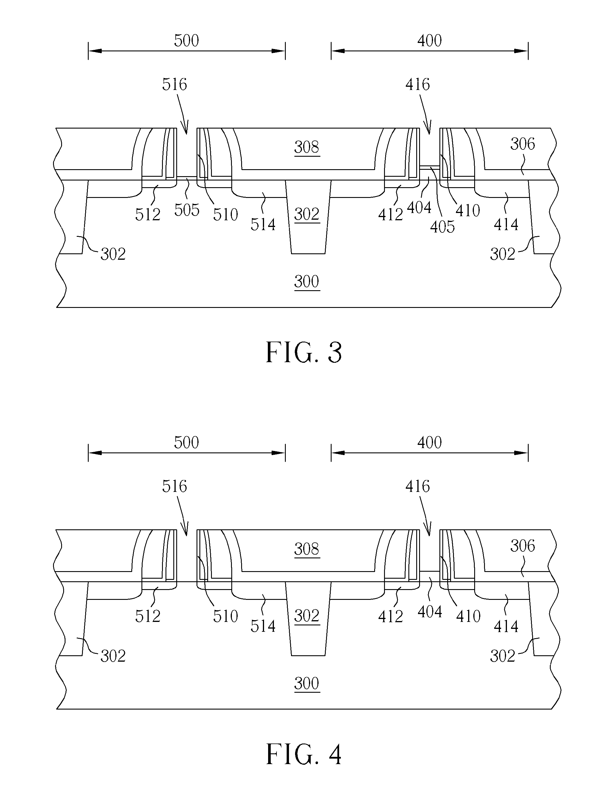
[0012]To provide a better understanding of the presented invention, preferred embodiments will be made in detail. The preferred embodiments of the present invention are illustrated in the accompanying drawings with numbered elements.

[0013]Please refer to FIG. 1 to FIG. 7, illustrating schematic diagrams of the method of fabricating a semiconductor device in the present invention. First, a substrate 300 is provided, such as a silicon substrate, an epitaxial silicon substrate, a silicon germanium substrate or a silicon-on-insulator (SOI). A plurality of shallow trench isolations (STI) 302 are disposed on the substrate 300. A first region 400 and a second region 500 are defined on the substrate 300. In one preferred embodiment, the first region 400 is a high-voltage device region such as an input / output region which contains high-voltage (1.8V or even higher) MOS transistors. The second region 500 is a low-voltage region such as a core region which contains low-voltage (0.9V or lower) ...


PUM


Abstract

The present invention provides a method of fabricating a semiconductor device. A substrate is provided. A first region and a second region are defined on the substrate. A first interfacial layer, a sacrifice layer and a sacrifice gate layer are disposed on the first region. The sacrifice layer and the sacrifice gate layer are disposed on the second region of the substrate. Next, a first etching step is performed to remove the sacrifice gate layer in the first region and the second region. Then, a second etching step is performed to remove the sacrifice layer in the first region and the second region to expose the substrate of the second region. Lastly, a second interfacial layer is formed on the substrate of the second region.

Description

BACKGROUND OF THE INVENTION[0001]1. Field of the Invention[0002]The present invention relates to a method of fabricating a semiconductor device, and more particularly, to a method of simultaneously forming a high-voltage device and a low-voltage device.[0003]2. Description of the Prior Art[0004]With a trend toward scaling down the size of semiconductor devices, the conventional poly-silicon gate has faced problems such as inferior performance due to boron penetration and unavoidable depletion effect which increases equivalent thickness of the gate dielectric layer, reduces gate capacitance, and worsens a driving force of the devices. Therefore, work function metals that are suitable for use as the high-k gate dielectric layer are used to replace the conventional poly-silicon gate to be the control electrode.[0005]The conventional metal gate methods are categorized into gate first processes and gate last processes. In a conventional gate first process, the annealing process for formi...

Claims


Application Information

Patent Timeline
IPC IPC(8): H01L21/28
CPCH01L29/495H01L29/4966H01L29/513H01L29/517H01L21/823857H01L29/6656H01L29/6659H01L29/7833H01L21/823462H01L29/66545
Inventor FU, SSU-ITSENG, I-MINGLIOU, EN-CHIUANTSAI, SHIH-HUNG
Owner UNITED MICROELECTRONICS CORP
Why Eureka
Try Eureka