Method for manufacturing touch panel and method for manufacturing display device provided with touch panel

Inactive Publication Date: 2012-09-27
SHARP KK
View PDF11 Cites 26 Cited by
  • Summary
  • Abstract
  • Description
  • Claims
  • Application Information

AI Technical Summary

Benefits of technology

[0026]By the method for manufacturing a touch panel according to one embodiment of the pr

Problems solved by technology

Therefore, this leads to an increase in the manufacturing costs and time needed for manufacturing a touch panel.
Further, an increase in the number of exposure masks means an increase in the number of t

Method used


Image

  • Method for manufacturing touch panel and method for manufacturing display device provided with touch panel
  • Method for manufacturing touch panel and method for manufacturing display device provided with touch panel
  • Method for manufacturing touch panel and method for manufacturing display device provided with touch panel

Examples


embodiment 1

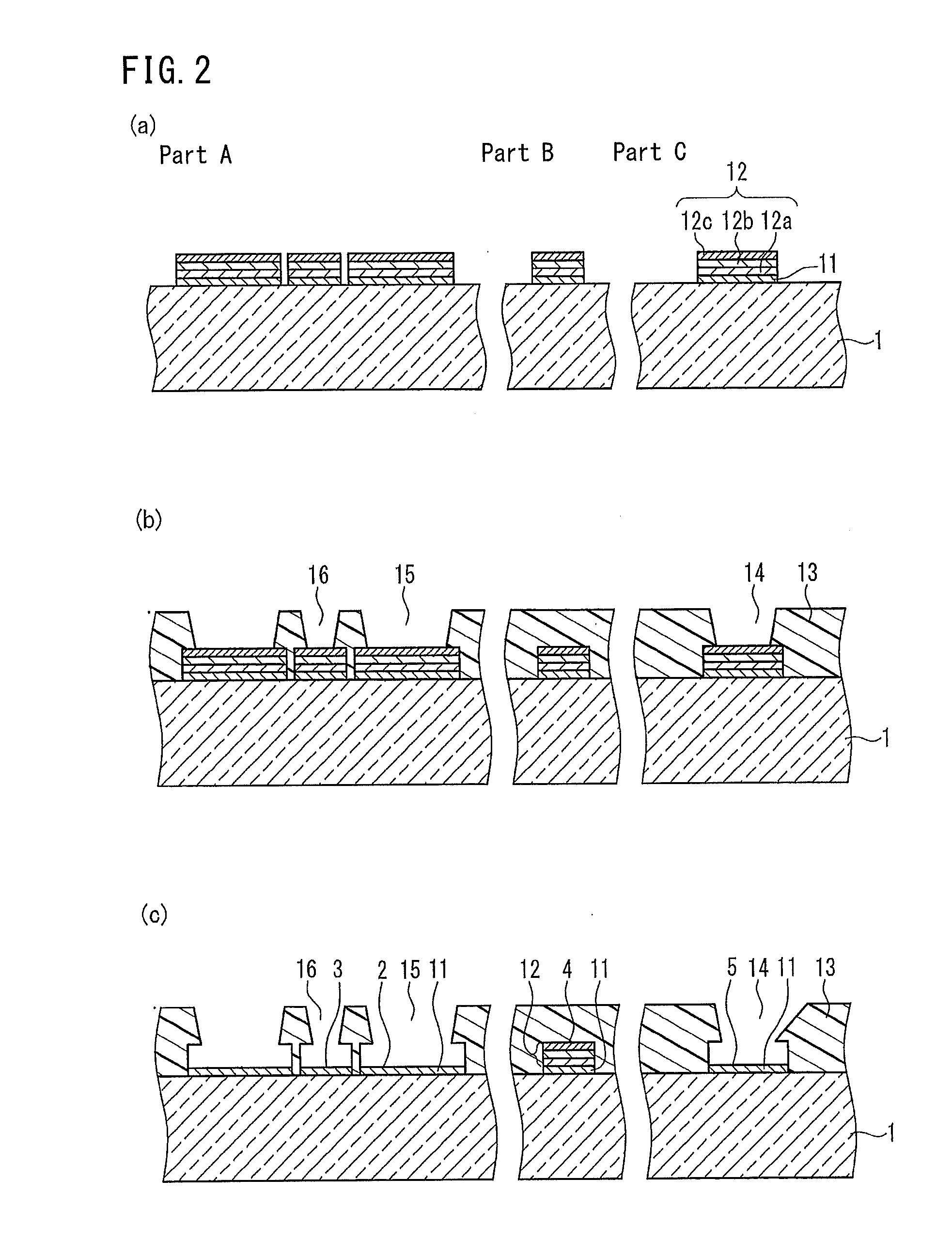
[0090]First, a method for manufacturing a touch panel in which touch electrodes, lead lines, and connection terminals are formed in one layer on a transparent substrate is explained as Embodiment 1.

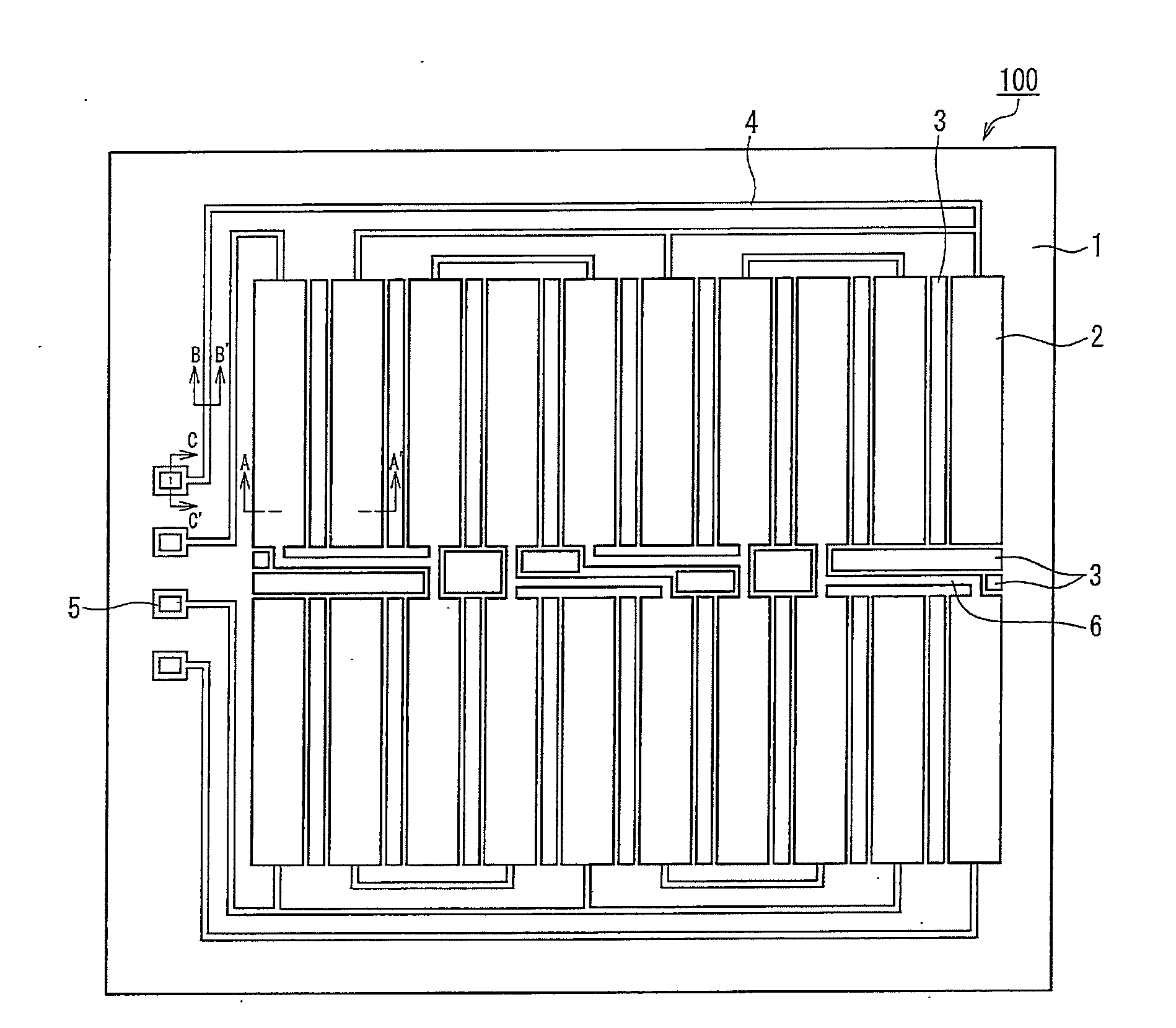
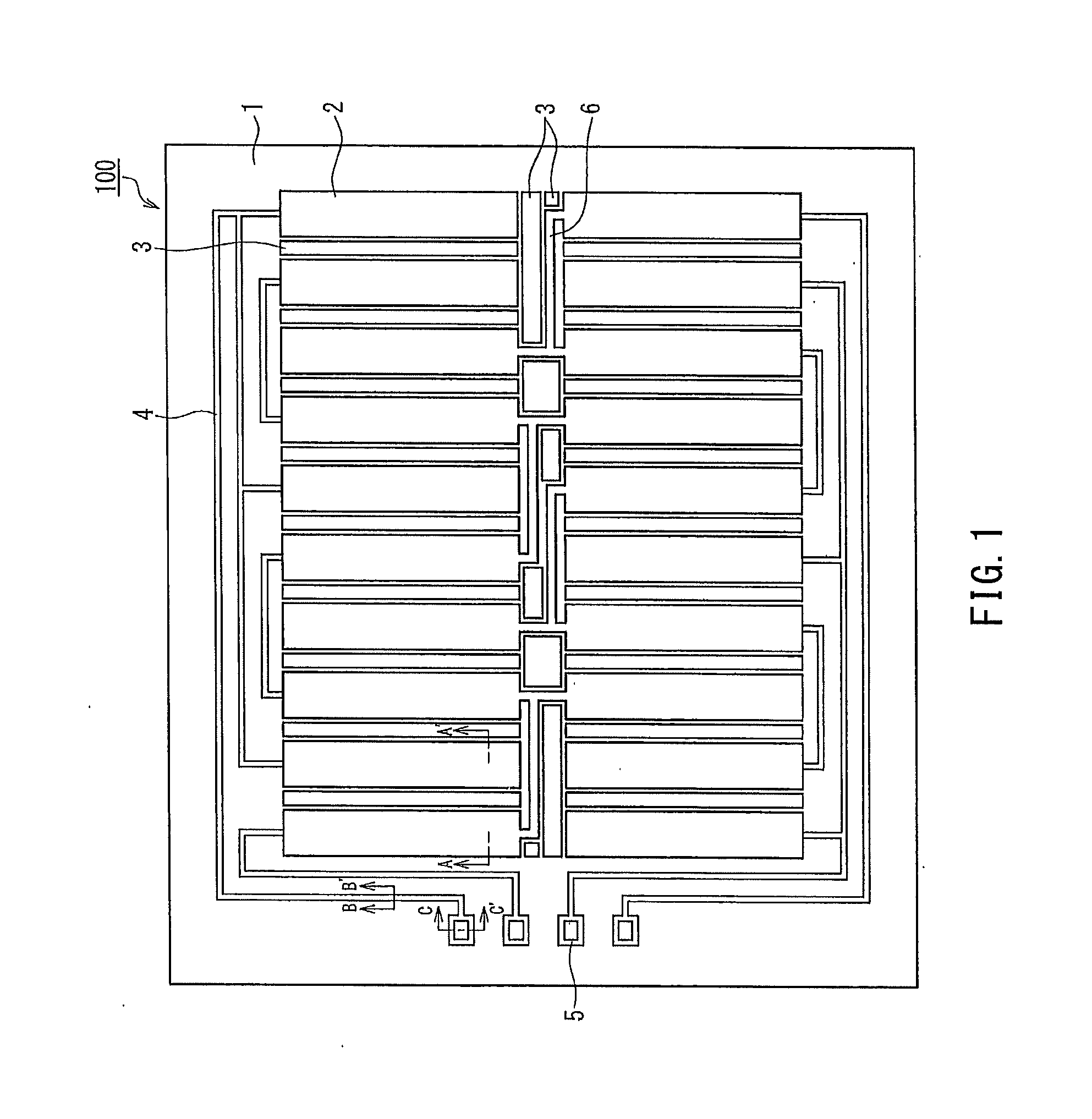
[0091]FIG. 1 is a plan view showing a touch electrode pattern in a touch panel 100 manufactured by a touch panel manufacturing method according to Embodiment 1.

[0092]In the touch panel 100, transparent conductive film layers made of ITO or the like are formed as two-dimensional patterns on a glass substrate 1 as an insulative transparent substrate, whereby touch electrodes 2 are formed thereon. Since the touch panel 100 of the present embodiment is a projection-type electrostatic capacitance touch panel, the touch electrodes 2 are formed in a manner such that a plurality of approximately-rectangular electrode patterns in the same size are arranged as shown in FIG. 1. In the touch panel of the present embodiment, ten of the electrode patterns are arrayed in a line in a horizontal direction...

embodiment 2

[0148]Next, a method for manufacturing a touch panel in which touch electrodes, lead lines, and connection terminals are formed in a two-layer structure on an insulative transparent substrate is explained as Embodiment 2.

[0149]FIG. 6 is a plan view showing electrode patterns of a touch panel 200 manufactured by a touch panel manufacturing method according to Embodiment 2.

[0150]In the touch panel 200, transparent conductive film layers made of ITO are formed as two-dimensional patterns on a glass substrate 101 as an insulative transparent substrate, whereby touch electrodes are provided. In the touch panel 200 of the present embodiment, touch electrodes 102a and 102b, lead lines 104a and 104b, and connection terminals 105a and 105b are formed in a two-layer structure in which they are divided into two layers vertically arranged. This is the point in which the present embodiment is different from the electrode patterns of the touch panel 100 according to Embodiment 1 shown in FIG. 1.

[...

embodiment 3

[0218]Next, Embodiment 3 of a touch panel manufacturing method is explained. The present embodiment relates to method for manufacturing a touch panel having a so-called rerouted line, that is, a touch panel in which touch electrodes and connection terminals are formed in one layer and at least a part of lead lines are rerouted and connected in a different layer than the layer in which the touch electrodes and connection terminals are formed.

[0219]FIG. 19 is a plan view showing electrode patterns of a touch panel 300 manufactured by the touch panel manufacturing method of the present embodiment.

[0220]The touch panel 300 includes touch electrodes 202 obtained by forming transparent conductive film layers made of ITO as two-dimensional patterns on a glass substrate 201 as an insulative transparent substrate. In the touch panel 300 of the present embodiment, the lead lines 204 for connecting the touch electrodes 202 and the connection terminals 205 are discontinued in the layer where th...


PUM

PropertyMeasurementUnit
Electrical conductoraaaaaaaaaa
Transparencyaaaaaaaaaa

Abstract

Provided is a touch panel manufacturing method wherein the number of exposure masks needed for pattern formation is reduced, and a method for manufacturing a display device provided with a touch panel. A transparent conductive film layer (11) and a metal layer (12) are laminated on a transparent substrate (1), and the transparent conductive film layer (11) and the metal layer (12) are formed into predetermined electrode patterns, with use of one resist pattern. A protective film (13) covering the transparent conductive film layer (11) and the metal layer (12) is formed, and openings (14, 15, and 16) are provided at predetermined positioned in the protective film (13). By etching with use of the protective film (13) having the openings (14, 15, and 16), the metal layer (12) is removed so that the transparent conductive film layer (11) is exposed, whereby at least either touch electrodes (2) or connection terminals (5) are formed.

Description

TECHNICAL FIELD[0001]The present invention relates to a method for manufacturing a touch panel having touch electrodes formed with transparent conductive films on an insulative transparent substrate, and to a method for manufacturing a display device provided with a touch panel.BACKGROUND ART[0002]Recently, with the spread of personal digital assistants (PDA), palm top computers, portable game equipment, etc., a touch panel formed on a transparent substrate has been used widely as an input means that can be combined with a display device.[0003]For example, in a liquid crystal display device as a touch-panel-equipped display device, a transparent touch panel is laminated on an image display surface of liquid crystal panel, and an image displayed on the liquid crystal panel can be viewed through the touch panel. Such a liquid crystal display device is configured so that when a surface of the touch panel on a viewed side, that is, a surface thereof on which display images on the liquid...

Claims


Application Information

Patent Timeline
IPC IPC(8): H05K3/06
CPCG02F1/1333G02F1/13338G02F2001/136231G06F2203/04103B32B2457/208B32B15/08B32B27/38B32B27/42B32B15/04G02F1/136231
Inventor MISAKI, KATSUNORI
Owner SHARP KK
Why Eureka
Try Eureka