Pumped pinned photodiode pixel array

a photodiode and array technology, applied in the field of complementary metal oxide (cmos) imagers, can solve the problems of limited charge handling capacity, and limited capacity of conventional pixels

Active Publication Date: 2012-09-27
SEMICON COMPONENTS IND LLC
View PDF1 Cites 36 Cited by
  • Summary
  • Abstract
  • Description
  • Claims
  • Application Information

AI Technical Summary

Problems solved by technology

These conventional pixels, however, have well capacities that are limited to the difference in potential between adjacent wells

Method used


Image

  • Pumped pinned photodiode pixel array
  • Pumped pinned photodiode pixel array
  • Pumped pinned photodiode pixel array

Examples


Embodiment Construction

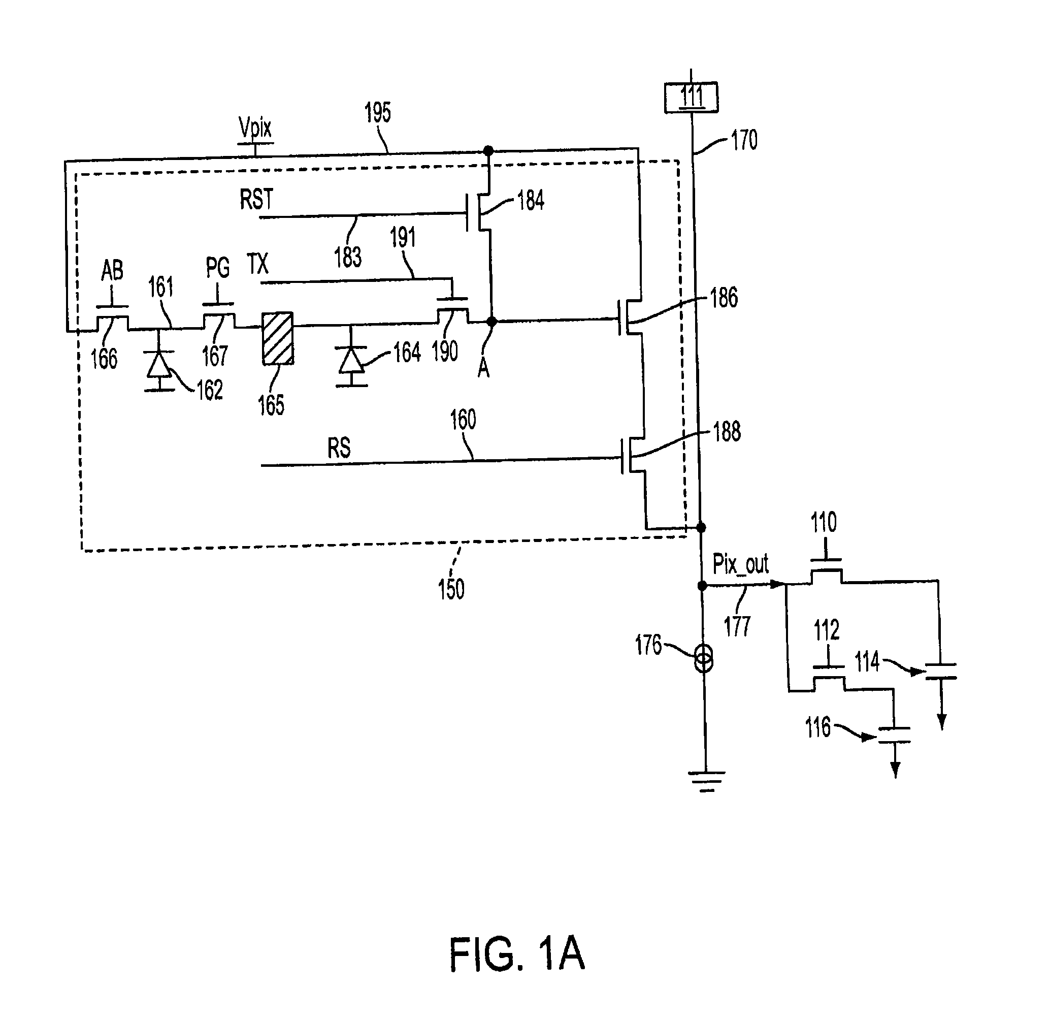
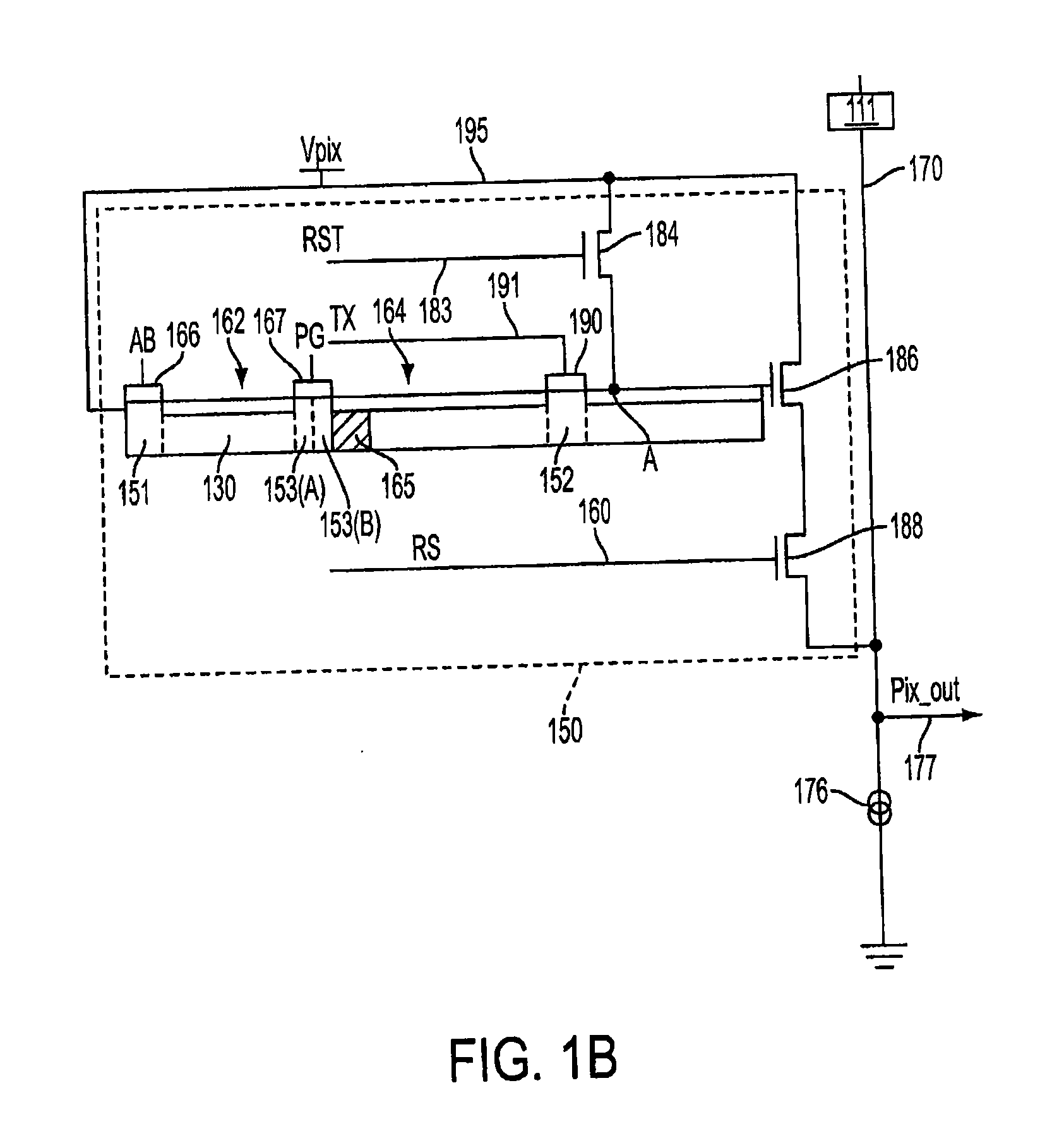
[0016]As described below, the present invention provides a pumped pixel having dual photo-diodes (e.g. pinned photo-diodes) and at least one virtual charge barrier (e.g. a heavily p-doped region on the surface and an n-doped region underneath). One of the photo-diodes accumulates charge in response to impinging photons. The other photo-diode acts as a memory node that stores the accumulated charge.

[0017]In one example, the accumulated charge is pumped (by a pump gate) over the charge barrier and into the photo-diode for storage or into the floating diffusion for readout. In general, the charge barrier blocks the charge from leaking back into the photo-diode from where it was pumped. Being able to pump and store the charge may allow the imager to delay pixel readout and / or extend dynamic range without the need for large voltage differences (differences in well potentials) and / or doping between the photo-diode wells.

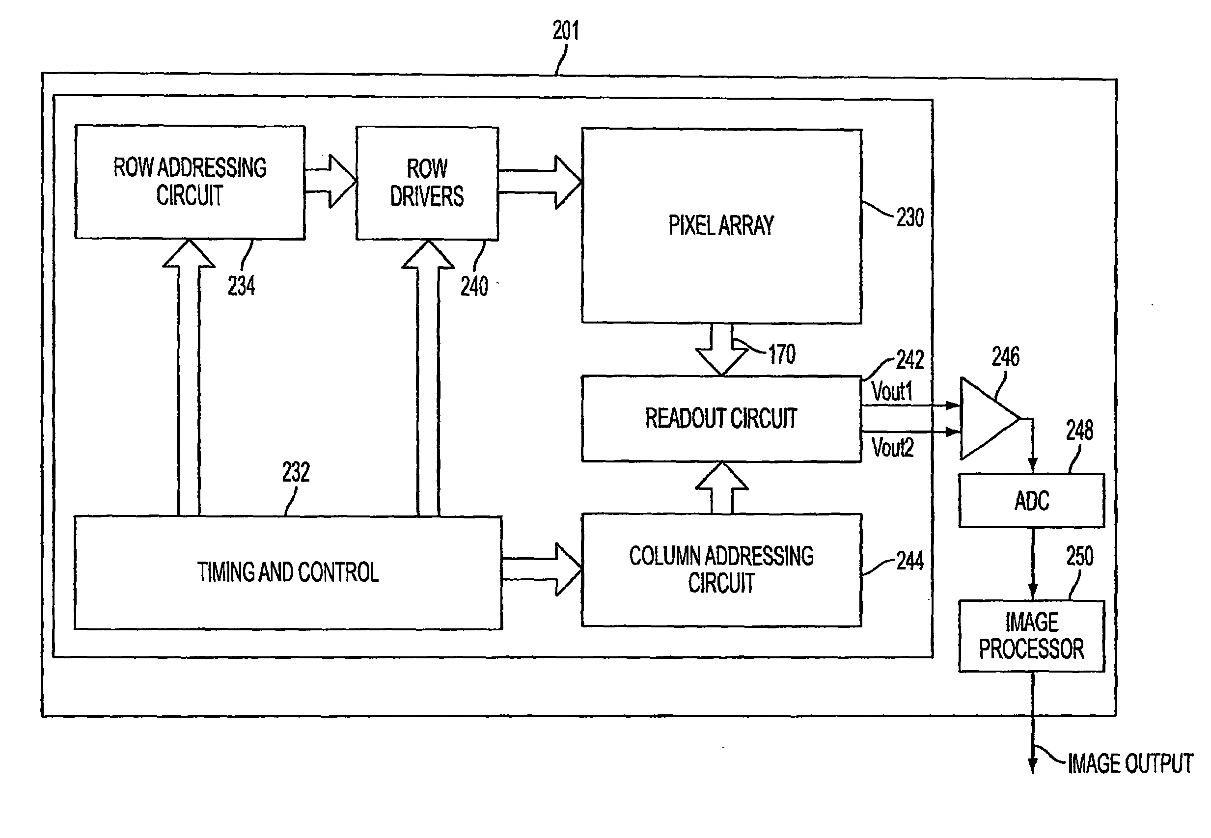
[0018]A six transistor (6T) circuit for a pixel 150 of a CMOS imager ...


PUM


Abstract

The present invention relates to a pumped pixel that includes a first photo-diode accumulating charge in response to impinging photons, a second photo-diode and a floating diffusion positioned on a substrate of the pixel. The pixel also includes a charge barrier positioned on the substrate between the first photo-diode and the second photo-diode, where the charge barrier temporarily blocks charge transfer between the first photo-diode and the second photo-diode. Also included is a pump gate positioned on the substrate adjacent to the charge barrier. The pump gate pumps the accumulated charge from the first photo-diode to the second photo-diode through the charge barrier in response to a pump voltage applied by a controller. Also included is a transfer gate positioned on the substrate between the second photo-diode and the floating diffusion. The transfer gate transfers the pumped charge from the second photo-diode to the floating diffusion in response to a transfer voltage applied by a controller.

Description

CROSS REFERENCE TO RELATED APPLICATIONS[0001]This application claims priority of U.S. Provisional Patent Application Ser. No. 61,467,561, filed Mar. 25, 2011, which is incorporated herein by reference.FIELD OF THE INVENTION[0002]The present invention relates, in general, to a complementary metal oxide (CMOS) imager that includes a plurality of pumped pixels for storing pixel charge before readout.BACKGROUND OF THE INVENTION[0003]In conventional dual pinned photo-diode pixels, one of the pinned photo-diodes is utilized as memory to store accumulated charge while reducing the effects of dark current. These conventional pixels, however, have well capacities that are limited to the difference in potential between adjacent wells. In general, a pinned photo-diode receiving charge must have a higher well potential than the well potential of a photo-diode supplying the charge. Charge transfer is performed similar to water transfer by pouring the charge from a lower well potential (shallow w...

Claims


Application Information

Patent Timeline
IPC IPC(8): H01L27/148H01L31/112
CPCH01L27/1461H01L27/14612H04N5/3532H04N5/37452H01L27/14887H01L27/14654H04N25/771H04N25/531
Inventor WAN, CHUNG CHUNLI, XIANGLI
Owner SEMICON COMPONENTS IND LLC
Why Eureka
Try Eureka