Low duty cycle distortion differential to CMOS translator

a translator and low duty cycle technology, applied in the field of electronic circuitry, can solve the problems of inconsistent delays, and achieve the effect of less reliance on transistor matching and simplified implementation

Active Publication Date: 2007-02-13
CYPRESS SEMICON CORP
View PDF6 Cites 31 Cited by
  • Summary
  • Abstract
  • Description
  • Claims
  • Application Information

AI Technical Summary

Benefits of technology

[0020]Alternatively, instead of using an inverter, the biasing circuit can simply be a transmission gate that, when enabled, resistively shorts the output of the inverter within the translator to its input. This will...

Problems solved by technology

Moreover, even if temperatures or voltages skew du...

Method used


Image

  • Low duty cycle distortion differential to CMOS translator
  • Low duty cycle distortion differential to CMOS translator
  • Low duty cycle distortion differential to CMOS translator

Examples


Embodiment Construction

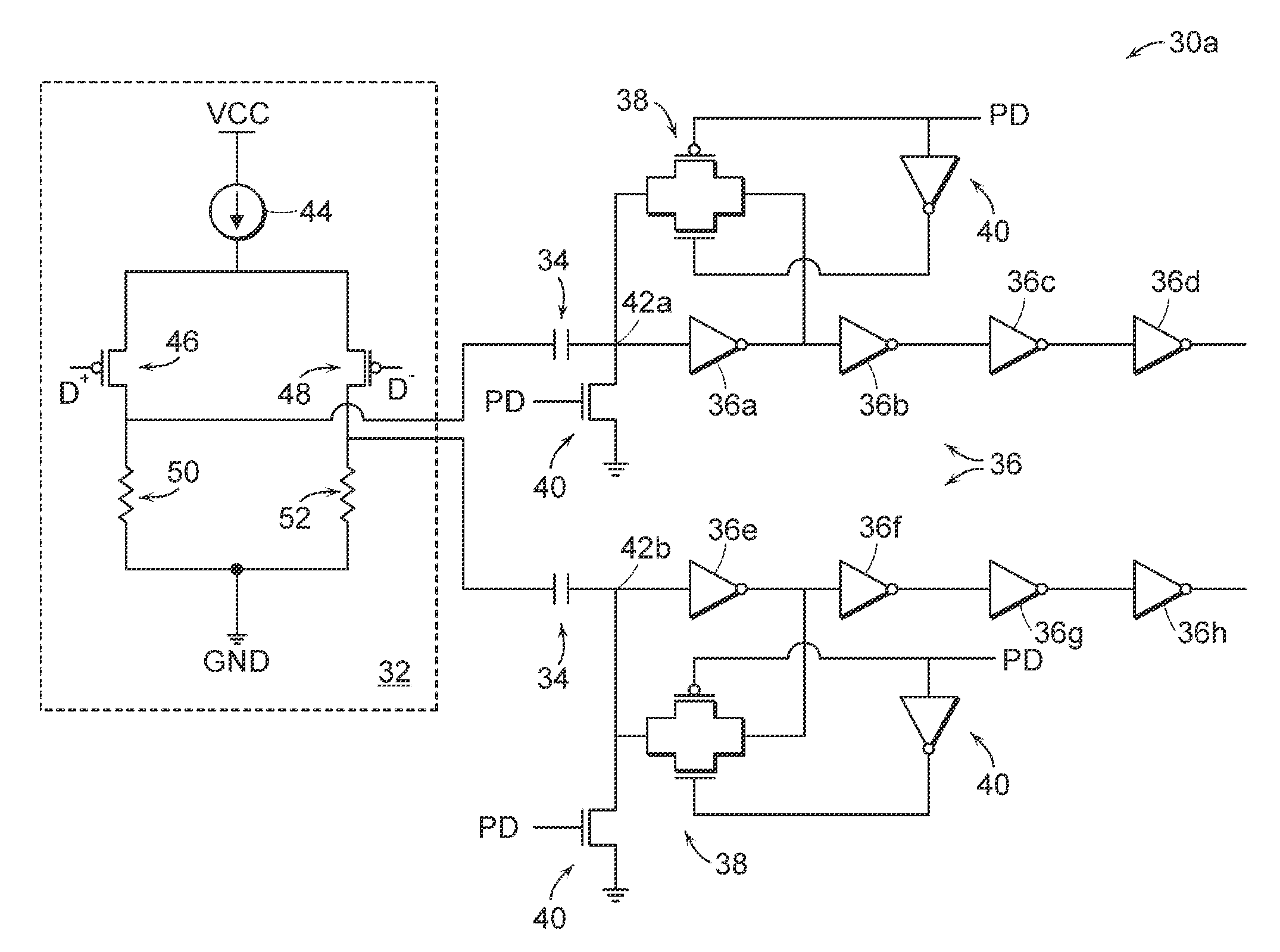
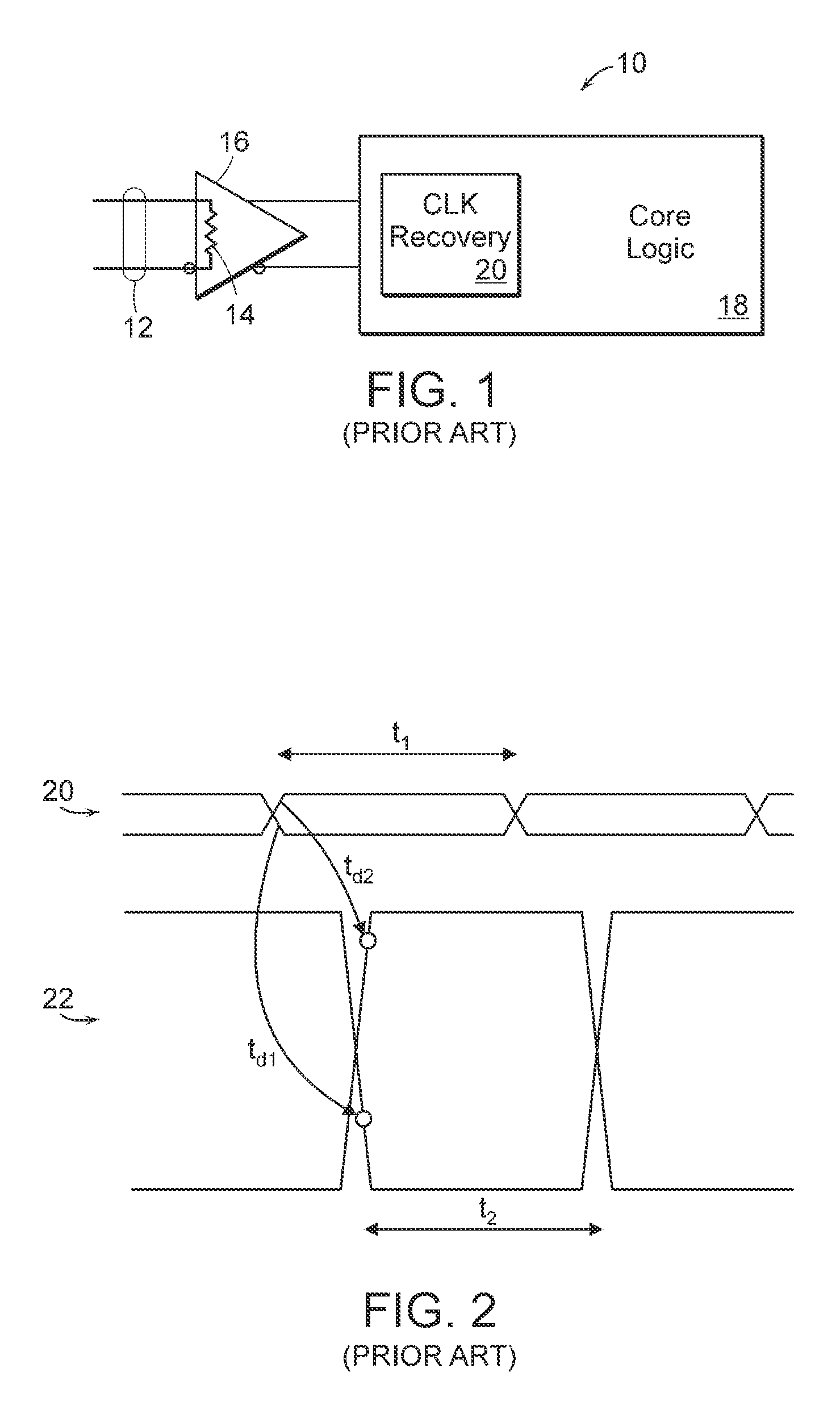
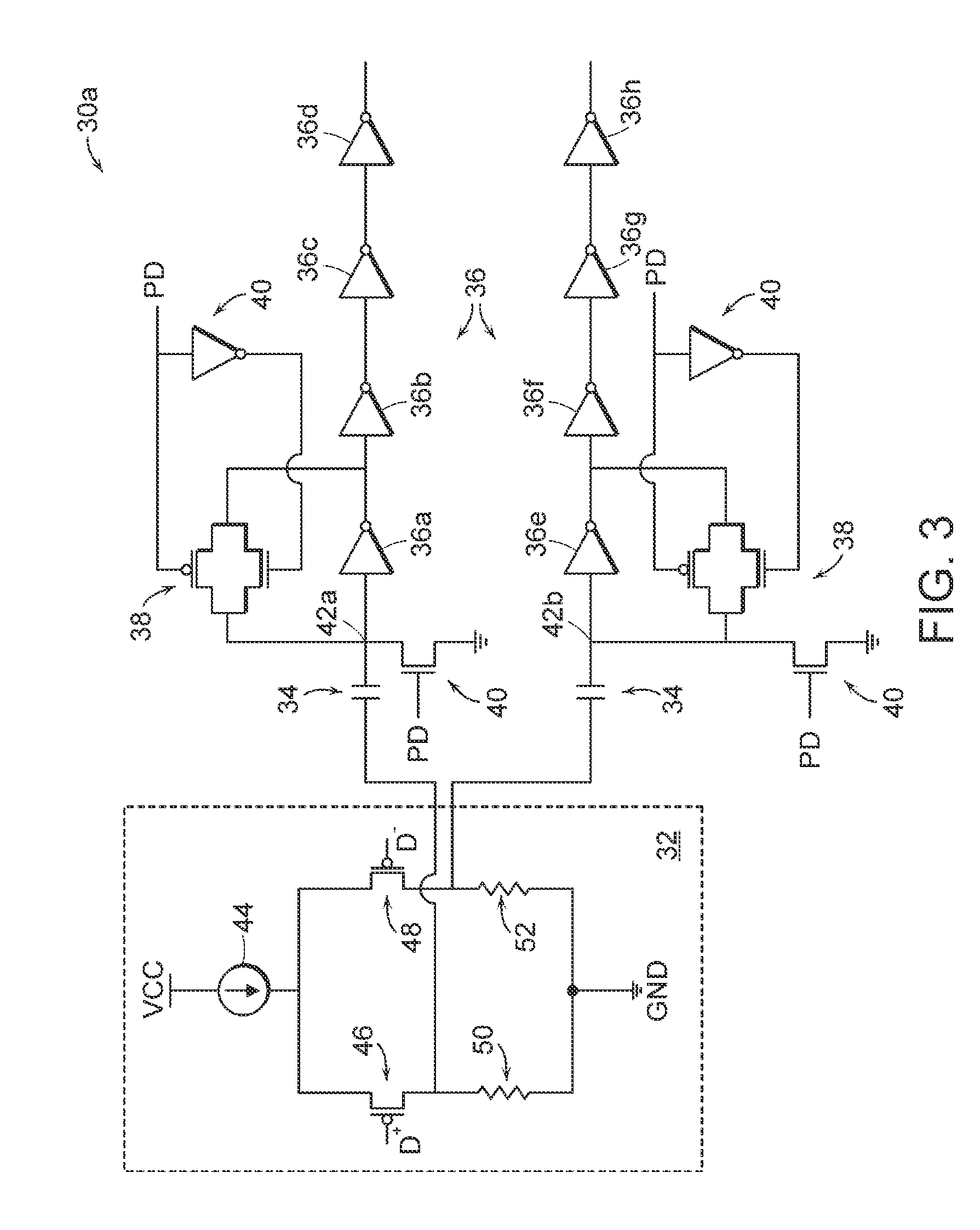
[0033]The importance of maintaining low amounts of duty cycle distortion within a translated differential signal is significant if that translated signal is used, for example, to accurately recover clock and data or translate a clock. Both the rising and falling edges of the incoming differential data stream is translated so that both edges have the same delay within the translator. By making the delay constant for the rising and falling edges on both the true and complementary translator outputs for all edges of the incoming differential signal, little if any jitter will occur and duty cycle distortion will be significantly low and, basically, nonexistent. Those jitter-free edges can then be used in latches of, for example, a digital phase-locked loop (PLL) to sample centers of the incoming signal.

[0034]The PLL can then be used, depending on which edge has arrived upon the latch, to pick a corresponding phase from, for example, a voltage-controlled oscillator (VCO). The digital PLL...


PUM


Abstract

Disclosed is a circuit comprising a differential input amplifier stage, a capacitor stage, an inverter chain stage, and a biasing circuit. The inverter chain stage may be formed with or without feedback depending on whether a clock signal or data signal is to be translated using the disclosed circuit. The biasing circuit can be formed using either inverters or transmission gates. Moreover, the biasing circuit, the inverter chain stage, and the amplifier stage can be connected to a power down circuit which, when the translator is not being used, will ensure various circuitry of the translator will not consume extensive power. The inverter chain stage, biasing circuit, and capacitor stage are formed on both an upper and lower section to produce true and complementary outputs that have a consistent and equal delay from the transitions of the incoming differential input signal so as to minimize jitter and associated duty cycle of the translated output.

Description

PRIORITY APPLICATION[0001]This application claims priority to provisional application No. 60 / 454,965 entitled “Low Duty Cycle Distortion Differential to CMOS Transistor,” filed Mar. 14, 2003.BACKGROUND OF THE INVENTION[0002]1. Field of the Invention[0003]This invention relates generally to electronic circuitry and, more particularly, to translation of electronic signaling levels in integrated circuits.[0004]2. Description of the Related Art[0005]The following descriptions and examples are given as background information only.[0006]The transmission of data involves sending and receiving data over a transmission path, or transmission medium. The transmission medium is generally coupled between a pair of transceivers, each of which preferably has a receiver and a transmitter. The receiver receives data from the transmission medium, and the transmitter drives data onto the transmission medium.[0007]Numerous transmission protocols have been established for sending and receiving data acro...

Claims


Application Information

Patent Timeline
IPC IPC(8): H03K19/0175H03K3/45
CPCH03K19/018528
Inventor PRATHER, STEPHEN M.WALDRIP, JEFFREY F.BERZINS, MATTHEW S.CORNELL, CHARLES A.
Owner CYPRESS SEMICON CORP
Why Eureka
Try Eureka