Optical member, near infrared cut filter, solid-state imaging element, lens for imaging device, and imaging/display device using the same

a technology of optical components and lenses, applied in the direction of camera filters, instruments, television systems, etc., can solve the problems of hardly made thin, inability to meet, and high price of light absorbing glass filters, and achieve the effect of good near infrared shielding function, reduced thickness, and sufficient downsizing

Active Publication Date: 2012-09-27
ASAHI GLASS CO LTD
View PDF8 Cites 76 Cited by
  • Summary
  • Abstract
  • Description
  • Claims
  • Application Information

AI Technical Summary

Benefits of technology

[0046]According to the present invention, an optical member, a near infrared cut filter, a solid-state imaging element and a lens, which have good near infrared shielding function and which are ca...

Problems solved by technology

However, a light absorbing type glass filter is expensive and is hardly made thin, and it cannot satisfactory meet the demands for downsizing and reduction in thickness of imaging devices in recent years.
Further, a ghost is likely to occur by entrance of a reflected light as a stray light into the solid-state imaging element.
However, this film is not satisfactory in the near infrared shielding properties.
However, this filter is also not satisfactory in the near infrared shielding properties, and it cannot satisfactory meet the demands for downsizing and reduction in thickness.
However, with respect to the solid-state imaging device, the near infrared absorbing compound used has no sufficient effect to absorb light...

Method used


Image

  • Optical member, near infrared cut filter, solid-state imaging element, lens for imaging device, and imaging/display device using the same
  • Optical member, near infrared cut filter, solid-state imaging element, lens for imaging device, and imaging/display device using the same
  • Optical member, near infrared cut filter, solid-state imaging element, lens for imaging device, and imaging/display device using the same

Examples


first embodiment

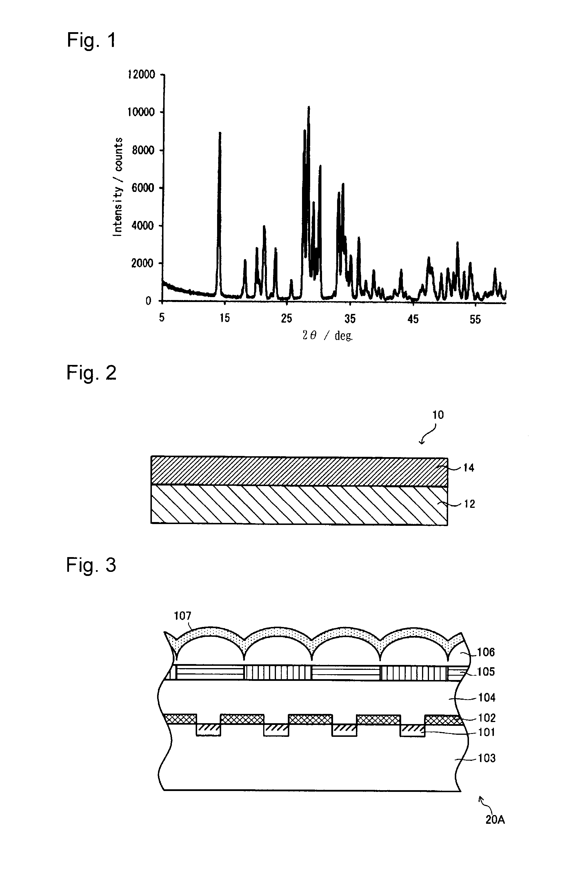
[0079]The first embodiment of the present invention relates to an optical member in the form of a film or a thin plate containing near infrared absorbing particles (hereinafter sometimes referred to as nIR absorbing particles).

[0080]The nIR absorbing particles used in this embodiment comprise crystallites of an oxide containing at least Cu and P and have a number average aggregated particle size of at least 20 nm and at most 200 nm, and preferably they comprise crystallites of a compound represented by the above formula (1) and have a number average aggregated particle size of at least 20 nm and at most 200 nm. By using the crystallites as an absorbing substance, near infrared absorbing properties resulting from the crystal structure can be maintained. Further, as the crystallites are fine particles, the absorbing substance can be contained in the optical member at a high concentration, and the absorbing ability per unit length can be increased.

[0081]In this specification, the follo...

second embodiment

[0159]The second embodiment of the present invention relates to a near infrared cut filter comprising a near infrared absorbing layer containing nIR absorbing particles on a transparent substrate surface. FIG. 2 is a cross-sectional view schematically illustrating a part of the near infrared cut filter according to this second embodiment. In the embodiment described hereinafter, in order to avoid repetition in a description, description of points common to the first embodiment is omitted in some cases, and differences will be mainly described.

[0160]As shown in FIG. 2, a near infrared cut filter 10 of this embodiment comprises a transparent substrate 12 and a near infrared absorbing layer 14 containing nIR absorbing particles formed on one side of the transparent substrate. The near infrared absorbing layer 14 may be formed also on the other side of the transparent substrate 12.

[0161]Hereinafter, the near infrared absorbing layer containing nIR absorbing particles will sometimes be r...

third embodiment

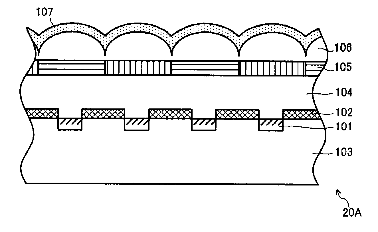
[0193]The third embodiment of the present invention relates to a solid-state imaging element comprising a near infrared absorbing layer containing near infrared absorbing particles. FIG. 3 is a cross-sectional view schematically illustrating a part of a solid-state imaging element according to this third embodiment. The solid-state imaging element of this embodiment is a solid-state imaging element to be used for an imaging device such as a miniature camera, to be installed in information equipment of e.g. a digital still camera, a digital video camera, a portable phone, a notebook personal computer or a PDA (personal digital assistant).

[0194]As shown in FIG. 3, in a solid-state imaging element 20A, on a semiconductor substrate 103 such as a silicon substrate having photoelectric conversion elements 101 and a light shielding layer 102 formed thereon, a planarizing layer 104, a color filter layer 105 and a microlens 106 are provided in this order. On the surface of the microlens 106,...


PUM


Abstract

Disclosed is an optical member in the form of a film or a thin plate. The optical member contains near infrared absorbing particles comprising crystallites of an oxide containing at least Cu and P and having a number average aggregated particle size of at least 20 nm and at most 200 nm. Further, a near infrared cut filter, a solid-state imaging element, a lens for an imaging device and an imaging/display device are disclosed. They comprise a near infrared absorbing layer containing near infrared absorbing particles comprising crystallites of an oxide containing at least Cu and P and having a number average aggregated particle size of at least 20 nm and at most 200 nm.

Description

TECHNICAL FIELD[0001]The present invention relates to an optical member in the form of a film or a thin plate having a near infrared shielding effect, a near infrared cut filter, a lens for an imaging device and a solid-state imaging element, and further relates to an imaging / display device using the same.BACKGROUND ART[0002]In recent years, in various applications, an optical filter or film through which light in the visible wavelength region (420 to 630 nm) is transmitted, but which blocks out light in the near infrared wavelength region (700 to 1,200 nm) has been used.[0003]For example, in an imaging device such as a digital still camera or a digital video camera employing a solid-stage imaging element (such as a CCD or a CMOS) or a display device such as an automatic exposure meter employing a light receiving element, in order to bring the sensitivity of the solid-state imaging element or the light receiving element closer to the visual sensitivity of the human, such an optical ...

Claims


Application Information

Patent Timeline
IPC IPC(8): G02B13/14
CPCG02B3/0056G02B5/201H04N5/2254G02B13/006G03B11/00G02B5/208H01L27/14621H01L27/14623H01L27/14627
Inventor OSAWA, MITSUOHASEGAWA, MAKOTOITO, WAKAKOZENG, HAISHENGABE, KEISUKE
Owner ASAHI GLASS CO LTD
Why Eureka
Try Eureka