Gap-Mode Waveguide

Active Publication Date: 2012-09-27
GIBONEY KIRK S
View PDF3 Cites 32 Cited by
  • Summary
  • Abstract
  • Description
  • Claims
  • Application Information

AI Technical Summary

Benefits of technology

[0050]s) A gap-mode waveguide may be constructed that is robust and performs with relatively high reliability over a lar

Problems solved by technology

Existing and proposed terahertz waveguide solutions are inadequate for many possible applications.
Dielectric waveguides of practical size do not support a low-loss, low-dispersion mode over broad bandwidths in the terahertz freq

Method used


Image

  • Gap-Mode Waveguide
  • Gap-Mode Waveguide
  • Gap-Mode Waveguide

Examples


Example

Example 1

FIGS. 3-9C

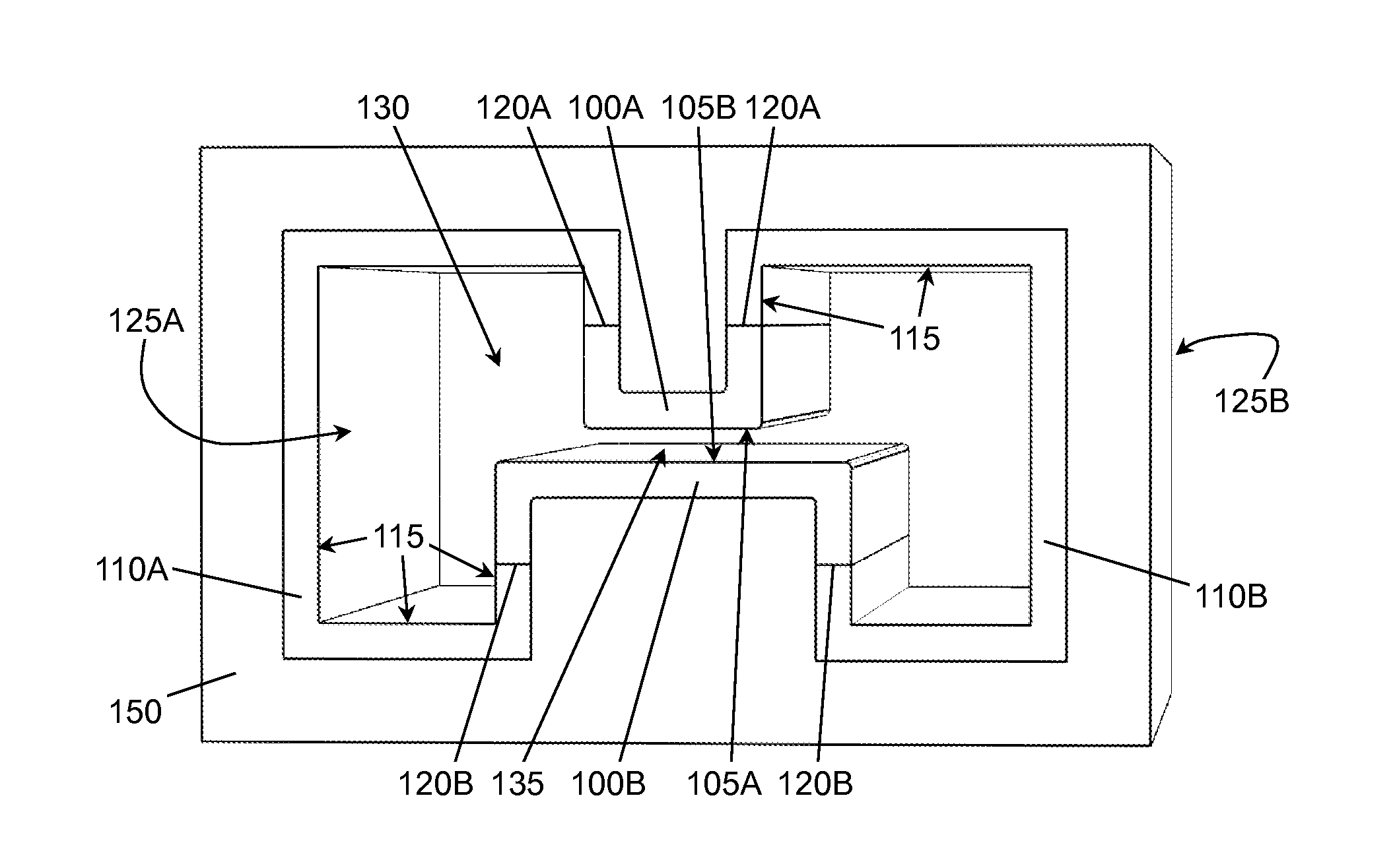
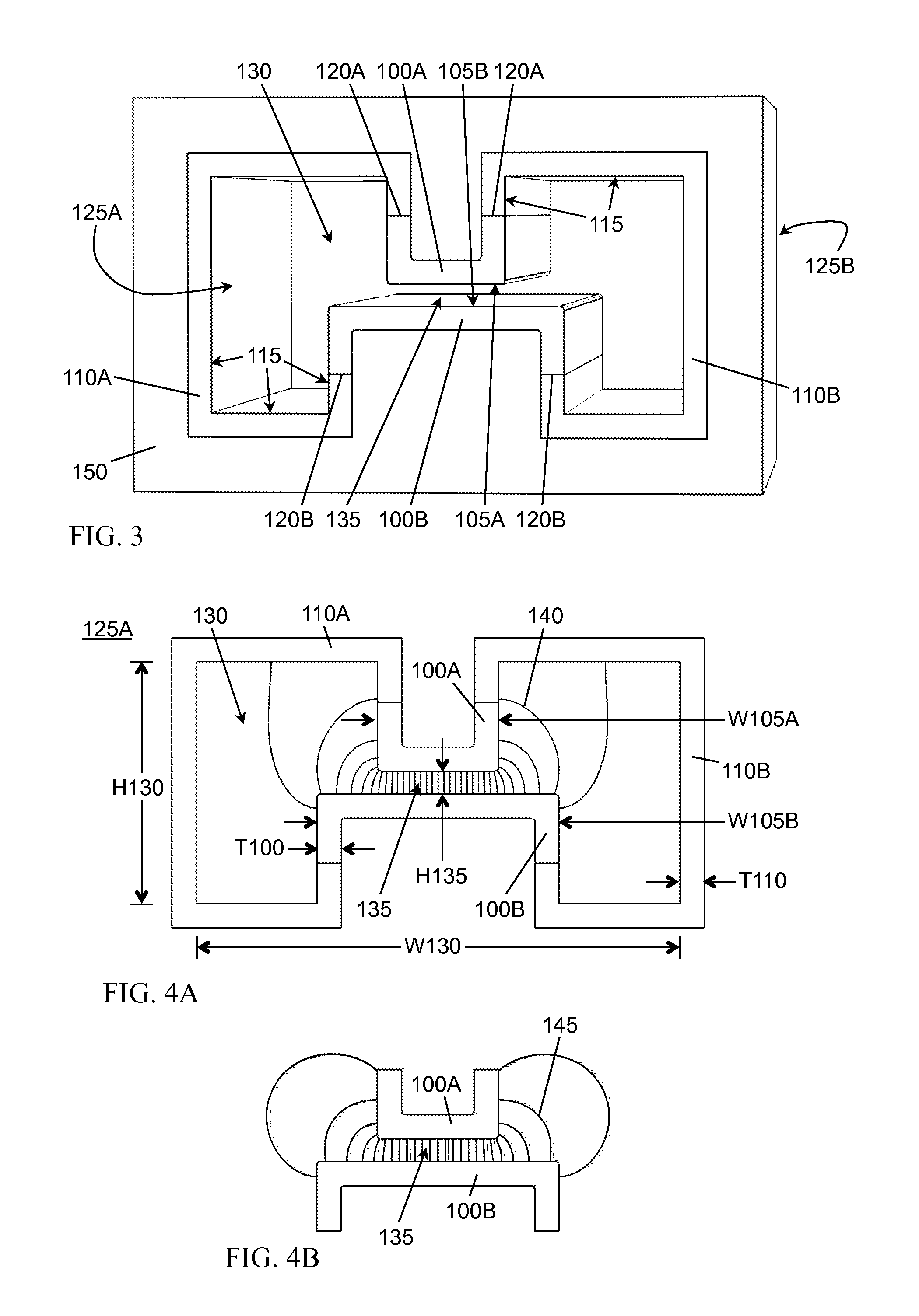
[0142]A gap-mode waveguide embodiment having a microstrip-like gap mode is illustrated by perspective view in FIG. 3 and by an elevation or end view in FIG. 4A. Two conductor walls, 100A and 100B, and two absorber walls, 110A and 110B, form the sides of the tubular waveguide. An interior gap 135 in the interior region 130 is formed between conductor walls proximate interior surface portions, 105A and 105B. The absorber walls, 110A and 110B, include absorber walls interior surfaces 115 that are adjacent the interior region 130. Ports, 125A and 125B, bound the ends of the waveguide. The conductor walls proximate interior surface portions, 105A and 105B, have generally parallel interior surfaces bordering the interior gap 135 as necessary for the propagation characteristics to remain within specified tolerances. The upper conductor wall gap-facing width W105A is narrower than the lower conductor wall gap-facing width W105B. The corners of the conductor walls, 100A an...

Example

Example 2

FIGS. 10-11B

[0199]This example provides for a change in propagation direction by bending or curving of a gap-mode waveguide, as illustrated in FIG. 10. A gap-mode electric-field-plane or E-plane bend 161 provides for a relatively low-loss change of the gap-mode propagation direction. As used in this specification and the attendant claims, the gap-mode electric-field plane is defined by the principal electric-field polarization and the propagation direction at a specified location, such as at a port or beginning of a bend, as in the present example. As used in this specification and the attendant claims, the principal electric-field polarization is defined as the polarization that best characterizes the overall gap-mode electric field. The principal electric-field polarization is generally the gap-mode electric field polarization at the center of the interior gap for gap-mode cross-sections having bilateral symmetry, as in the present example, or substantial bilateral symmet...

Example

Example 3

FIGS. 12-13B

[0204]This example describes a gap-mode waveguide embodiment having a twist, as illustrated in FIG. 12. A gap-mode waveguide twist 162 reorients the gap-mode electric field or E-field or principal electric-field polarization. A waveguide twist is a progressive rotation over distance of the waveguide cross-section about a twist axis parallel to the propagation direction. In an embodiment, non-axial points on a helical waveguide twist cross-section trace out helixes through the waveguide twist, and the waveguide cross-section is substantially constant through the twist. In another embodiment, one or more non-axial points on a non-helical waveguide twist cross-section do not trace out helixes through the waveguide twist, and the waveguide cross-section is not constant through the twist. The waveguide twist follows a specified twist rate versus propagation distance curve. The twist rate versus distance curve may be any curve that provides the prescribed change in pr...


PUM


Abstract

In a gap-mode waveguide embodiment, an interior gap in a tubular waveguide principally condenses a dominant gap mode near the interior gap, and an absorber dissipates electromagnetic energy away from the gap mode. In this manner, the gap mode may dissipate relatively little power in the absorber compared to other modes and propagate with lesser attenuation than all other modes. A gap mode launched into a gap-mode waveguide may provide for low-loss, low-dispersion propagation of signals over a bandwidth including a multimode range of the waveguide. Gap-mode waveguide embodiments of various forms may be used to build guided-wave circuits covering broad bandwidths extending to terahertz frequencies.

Description

CROSS-REFERENCES TO RELATED APPLICATIONS[0001]This application claims the benefit of U.S. Provisional Patent Application Ser. No. 61 / 466,343, filed 2011 Mar. 22, by the present inventor.DESCRIPTIONBackground Art[0002]The background art discussed in this section includes information disclosed under 37 CFR §1.97 and §1.98.[0003]Existing and proposed terahertz waveguide solutions are inadequate for many possible applications. Dominant mode loss of metallic tubular and multiconductor waveguides becomes very large as dimensions are scaled for single-mode operation at terahertz frequencies. Dielectric waveguides of practical size do not support a low-loss, low-dispersion mode over broad bandwidths in the terahertz frequency range. While some prior art multimode and mode-selective waveguides have offered promise of improvements in some aspects, they have failed to deliver a satisfactory combination of attributes for many practical applications.SUMMARY OF INVENTIONTechnical Problem[0004]Wha...

Claims


Application Information

Patent Timeline
IPC IPC(8): G02B6/12
CPCH01P1/162H01P3/123G01R1/24H01P1/042H01P5/024H01P1/02H01P1/165
Inventor GIBONEY, KIRK S.
Owner GIBONEY KIRK S
Why Eureka
Try Eureka