Pixel array of fringe field switching liquid crystal display panel and driving method thereof

a fringe field switching and liquid crystal display panel technology, applied in static indicating devices, instruments, non-linear optics, etc., can solve the problems of high power consumption of driving the array substrate, complicated driving methods of the array substrate, and driving up the cost of integrated circuits (ics), so as to improve the power consumption of the fringe field switching liquid crystal display panel, simplify the driving method, and reduce the cost of driving ics

Active Publication Date: 2012-10-04
AU OPTRONICS CORP
View PDF11 Cites 22 Cited by
  • Summary
  • Abstract
  • Description
  • Claims
  • Application Information

AI Technical Summary

Benefits of technology

[0007]In the pixel array of the fringe field switching liquid crystal display panel, the common lines, which may be driven independently, are employed with the allocation approaches of the common electrodes in the sub-pixel regions for presenting a dot inversion driving effect by a simplified driving method. Costs of the driving ICs may then be reduced, and the power consumption of the fringe field switching liquid crystal display panel may be also improved.

Problems solved by technology

However, in conventional fringe field switching liquid crystal display panels, a plurality of common lines, which connect to the common electrodes, are electrically connected to each other and may not be driven independently.
Therefore, driving methods of the array substrate have to be more complicated for presenting different display driving effects, such as a dot inversion driving effect.
This results in driving up the cost of integrated circuits (ICs) and high power consumption for driving the array substrate, also leads away from goals of energy saving and carbon reduction.

Method used


Image

  • Pixel array of fringe field switching liquid crystal display panel and driving method thereof
  • Pixel array of fringe field switching liquid crystal display panel and driving method thereof
  • Pixel array of fringe field switching liquid crystal display panel and driving method thereof

Examples


Embodiment Construction

[0017]To provide a better understanding to skilled users in the technology, the embodiments will be detailed as follows. The embodiments are illustrated in the accompanying drawings with numbered elements to elaborate the contents and effects to be achieved.

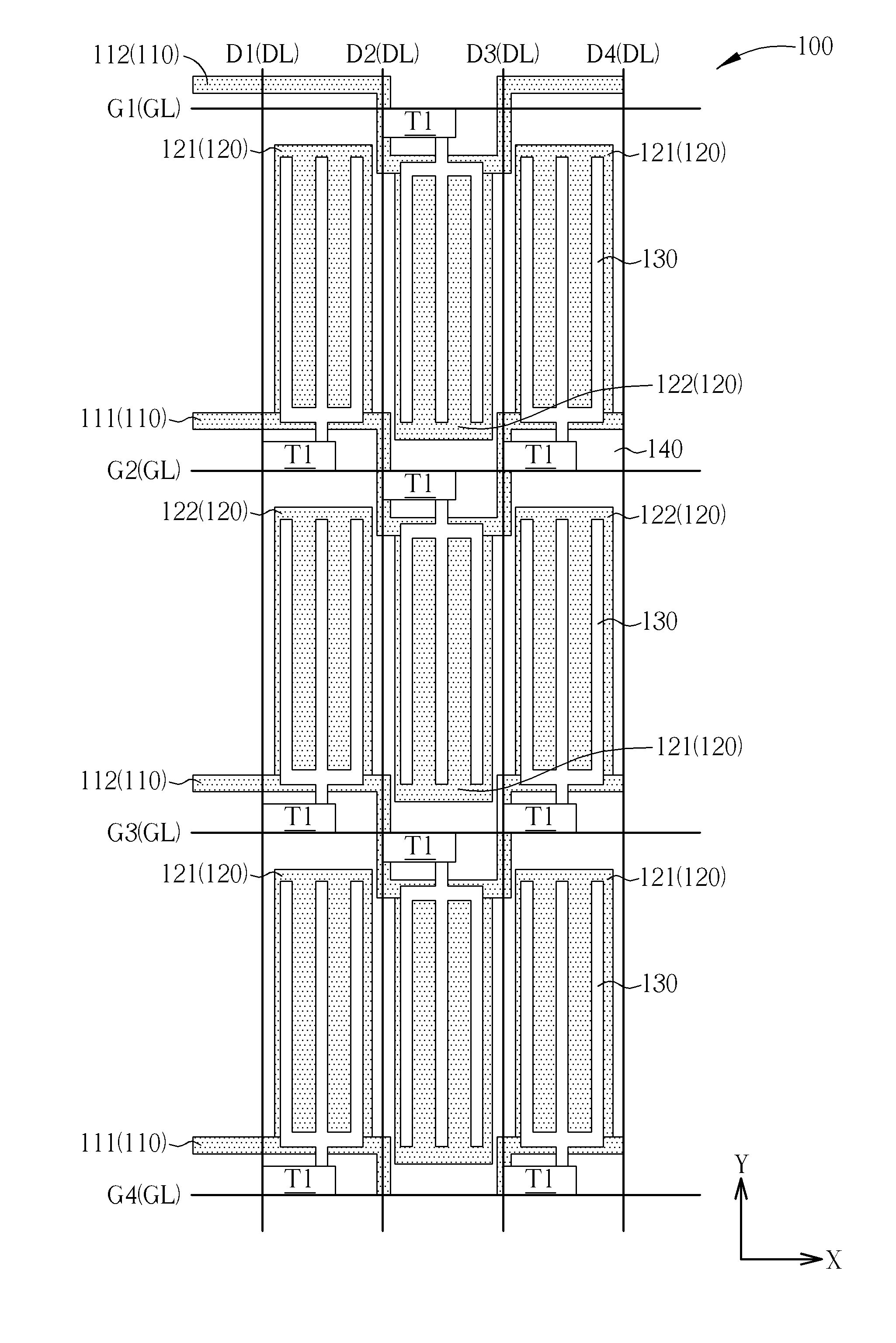
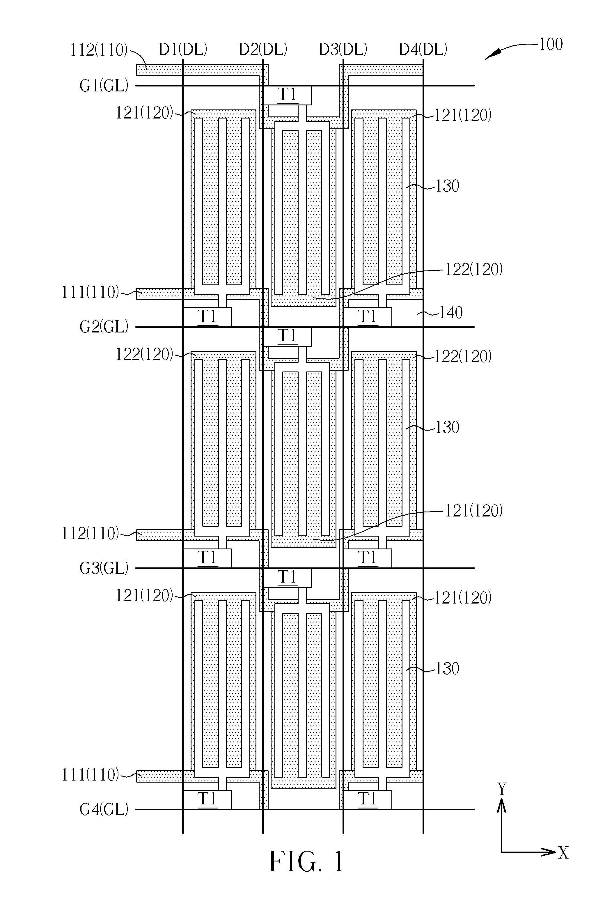
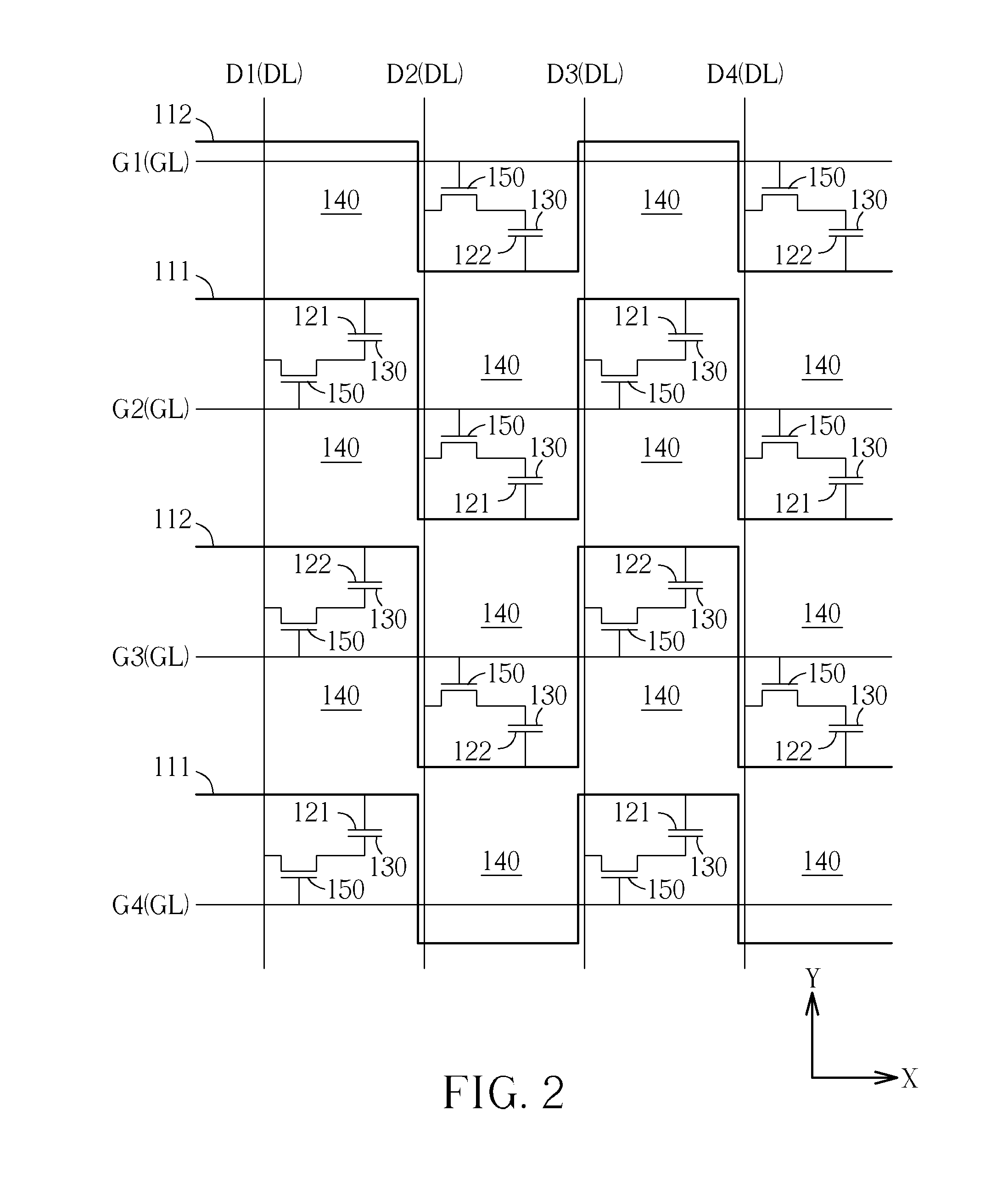
[0018]Please refer to FIGS. 1-3. FIG. 1 is a schematic diagram illustrating a pixel array of a fringe field switching liquid crystal display panel according to an embodiment. FIG. 2 is a schematic diagram illustrating electrical circuits of the pixel array of the fringe field switching liquid crystal display panel according to this embodiment. FIG. 3 is a schematic diagram illustrating common lines and common electrodes of the fringe field switching liquid crystal display panel according to this embodiment. Please note that the figures are only for illustration and the figures may not be to scale. The scale may be further modified according to different design considerations. As shown in FIG. 1, in this embodiment, a pixel array ...


PUM

PropertyMeasurementUnit
transparent conductiveaaaaaaaaaa
frame timeaaaaaaaaaa
electrical fieldaaaaaaaaaa

Abstract

A pixel array of a fringe field switching (FFS) liquid crystal display panel includes a plurality of gate lines, a plurality of data line, a plurality of pixel electrodes, and a plurality of common lines. The gate lines are disposed parallel to each other along a first direction. The data lines are disposed parallel to each other along a second direction. A plurality of sub-pixel regions is defined by the gate lines and the data lines. The common lines are disposed along the first direction and electrically isolated from each other. Each of the common lines includes a plurality of common electrodes extending along the second direction. The two adjacent common electrodes of each common line are respectively disposed in the two adjacent sub-pixel regions which are located in different rows.

Description

BACKGROUND[0001]1. Technical Field[0002]The disclosure relates to a pixel array of a fringe field switching liquid crystal display panel and a driving method thereof, and more particularly, to a pixel array of a fringe field switching liquid crystal display panel with a plurality of common lines and a driving method thereof.[0003]2. Description of Related Art[0004]Liquid crystal display panels are applied in many kinds of consumer electronics such as flat TVs, laptop computers, and cell phones. Fringe field switching (FFS) liquid crystal display panels have been developed for improving narrow viewing angle issues in liquid crystal display panels. The main features of the FFS liquid crystal display panel include that common electrodes and pixel electrodes are disposed in different layers of an array substrate (also called a thin film transistor substrate), and a wide viewing angle effect may be achieved by an electrical field generated by the common electrode and the pixel electrode....

Claims


Application Information

Patent Timeline
Patent Type & Authority Applications(United States)
IPC IPC(8): G02F1/1343
CPCG02F2001/134372G09G2310/08G09G2330/021G02F1/134363G09G3/3655G02F2201/121G09G2300/0426G09G3/3648G09G3/3614G02F1/134372
Inventor PAI, CHENG-CHIU
Owner AU OPTRONICS CORP
Why Eureka
Try Eureka