Method of manufacturing semiconductor light emitting device and mask for application of paste used therefor

Inactive Publication Date: 2012-10-04
SAMSUNG ELECTRONICS CO LTD
View PDF3 Cites 7 Cited by
  • Summary
  • Abstract
  • Description
  • Claims
  • Application Information

AI Technical Summary

Benefits of technology

[0007]An aspect of the present invention provides a method of manufacturing a semiconductor light emitting device, having enhanced precision and

Problems solved by technology

Here, a wire bonding pad may be polluted with a resin in a phosphor application process, causing a defective connection of a wire.
Further, in a case in which a phosphor layer having a nonuniform thickness is applied to a chip surface,

Method used


Image

  • Method of manufacturing semiconductor light emitting device and mask for application of paste used therefor
  • Method of manufacturing semiconductor light emitting device and mask for application of paste used therefor
  • Method of manufacturing semiconductor light emitting device and mask for application of paste used therefor

Examples


Embodiment Construction

[0041]Embodiments of the present invention will now be described in detail with reference to the accompanying drawings such that they could be easily practiced by those having skill in the art to which the present invention pertains. However, in describing the embodiments of the present invention, detailed descriptions of well-known functions or constructions will be omitted so as not to obscure the description of the present invention with unnecessary detail.

[0042]In addition, like reference numerals denote like elements throughout the drawings.

[0043]Unless explicitly described to the contrary, the word “comprise” and variations such as “comprises” or “comprising,” will be understood to imply the inclusion of stated elements but not the exclusion of other elements.

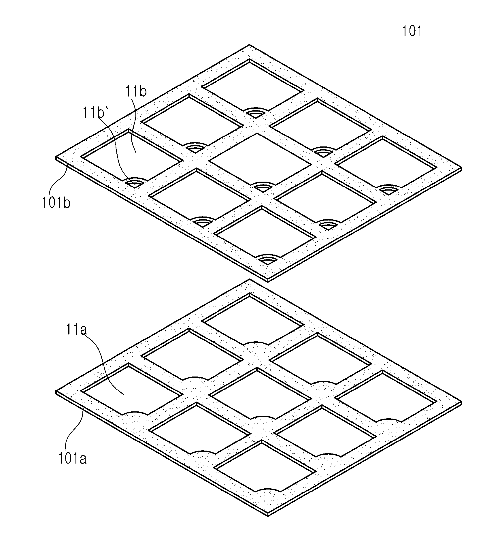
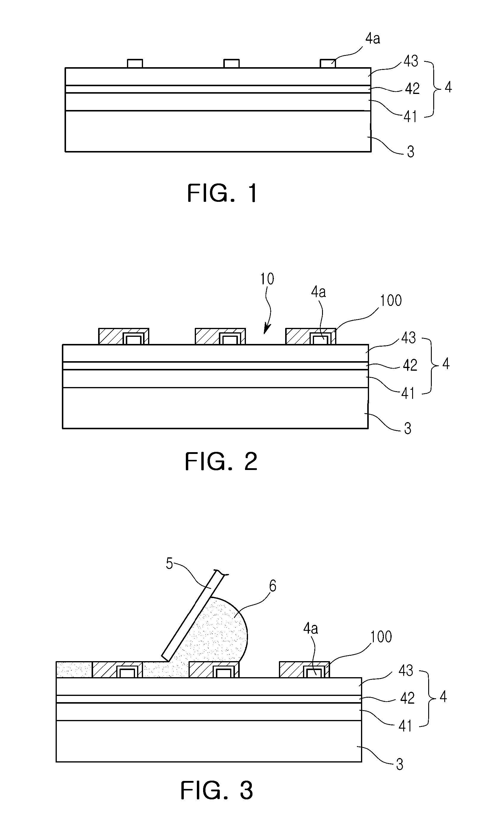
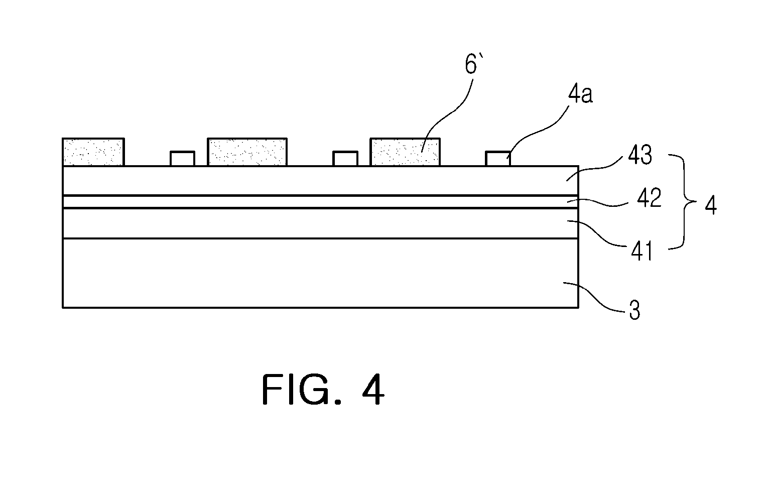
[0044]FIGS. 1 to 4 are schematic cross-sectional views showing a method of manufacturing a semiconductor light emitting device according to an embodiment of the present invention. According to the embodiment of the presen...


PUM


Abstract

Provided are a mask for an application of paste and a method of manufacturing a semiconductor light emitting device by using the same. The method includes preparing a light emitting structure including first and second conductive semiconductor layers and an active layer disposed therebetween, which has at least one electrode formed on a surface of the light emitting structure; disposing a mask having an open part exposing a portion of the surface of the light emitting structure therethrough and a recess part corresponding the electrode in a region thereof on a surface of the light emitting structure; and applying wavelength conversion material-containing paste to the surface of the light emitting structure through the open part.

Description

CROSS-REFERENCE TO RELATED APPLICATIONS[0001]This application claims the priority of Korean Patent Application No. 10-2011-0028308 filed on Mar. 29, 2011, in the Korean Intellectual Property Office, the disclosure of which is incorporated herein by reference.BACKGROUND OF THE INVENTION[0002]1. Field of the Invention[0003]The present invention relates to a method of manufacturing a semiconductor light emitting device and a mask for an application of paste used therefor.[0004]2. Description of the Related Art[0005]In general, a light emitting diode (LED) is a device used for transmitting a signal converting electrical energy into infrared rays, visible rays, or another form of light, by using compound semiconductor properties. The LED produces electroluminescence (EL), and an LED using a group III-V compound semiconductor is currently in practical use. The group III nitride-based compound semiconductor is a direct transition type semiconductor, which may perform a stabilized operation...

Claims


Application Information

Patent Timeline
IPC IPC(8): H01L33/50B05C11/00
CPCH01L33/38H01L2933/0041H01L33/505H01L33/50
Inventor YOO, CHEOL JUNHONG, SEONG JAE
Owner SAMSUNG ELECTRONICS CO LTD
Why Eureka
Try Eureka