Wafer shape thickness and trench measurement

a technology of trench measurement and wafer shape, applied in the field of optical measuring devices and methods, can solve the problem of no prior art that places the optics of reflectometers in one leg of michelson interferometers

Active Publication Date: 2012-10-11
ONTO INNOVATION INC
View PDF15 Cites 46 Cited by
  • Summary
  • Abstract
  • Description
  • Claims
  • Application Information

AI Technical Summary

Benefits of technology

[0049]OCT systems are designed for biological specimens consisting of weakly scattering objects, such as cells, with little a priori information regarding their location in any of the three dimensions. The present invention is intended specifically for test objects that consist of distinct layers of homogeneous media. These layers may include silicon wafers such as carrier wafers and product wafers, as w

Problems solved by technology

However, we know of no prior art that places the reflectometer optics in one leg of a Michelson interferometer, or t

Method used


Image

  • Wafer shape thickness and trench measurement
  • Wafer shape thickness and trench measurement
  • Wafer shape thickness and trench measurement

Examples


Embodiment Construction

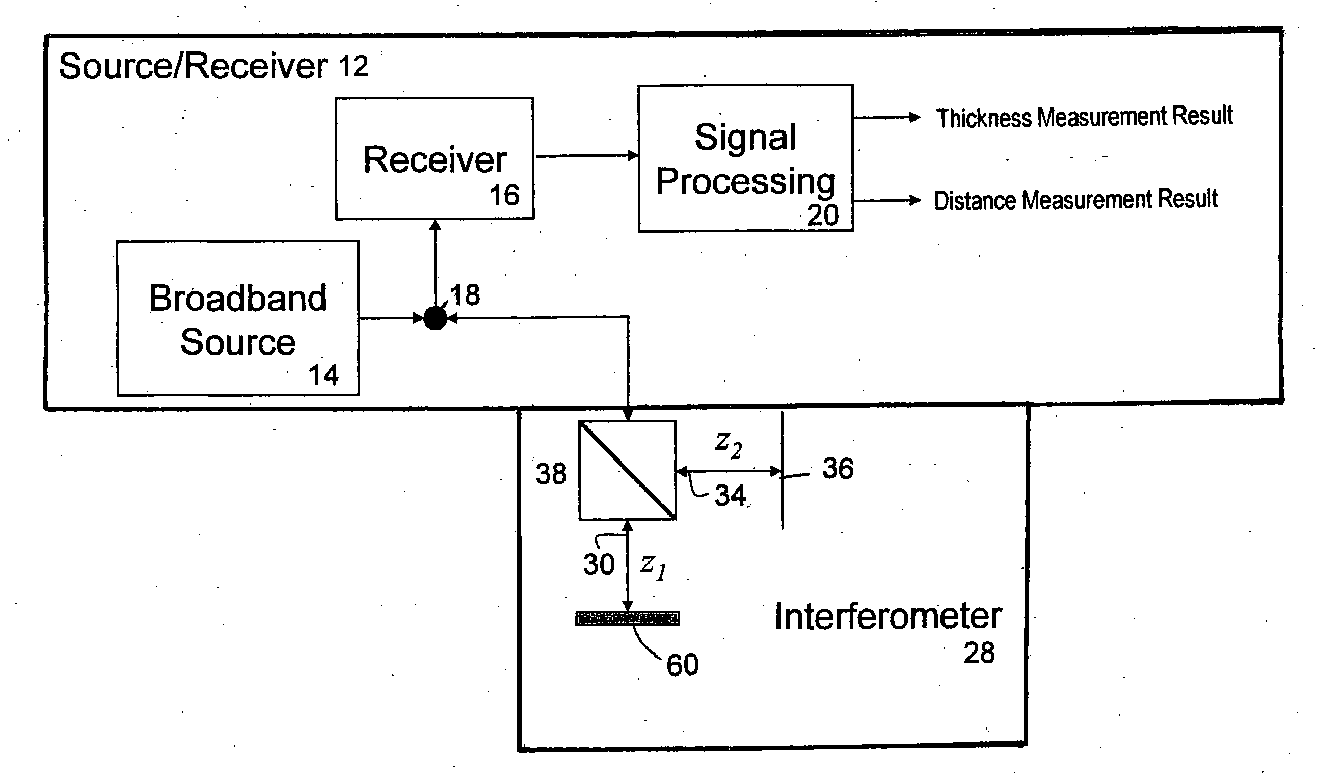
[0059]The best mode for carrying out the invention is presented in terms that disclose a device and methods for measuring the thickness of, the shape of, and the depth of etched features on a wafer.

[0060]The invention combines a Michelson interferometer which is used for distance measurements, with a reflectometer which is used for thickness measurements. While Michelson interferometers and reflectometers are each well known in the art, their combination for the purpose of simultaneous shape and thickness measurements is novel. Furthermore, the successful implementation of this optical architecture compels specific requirements for the optical source, the signal processing, and system methods. This disclosure discusses the optical physics, the signal processing, optical source requirements, and system level implementation.

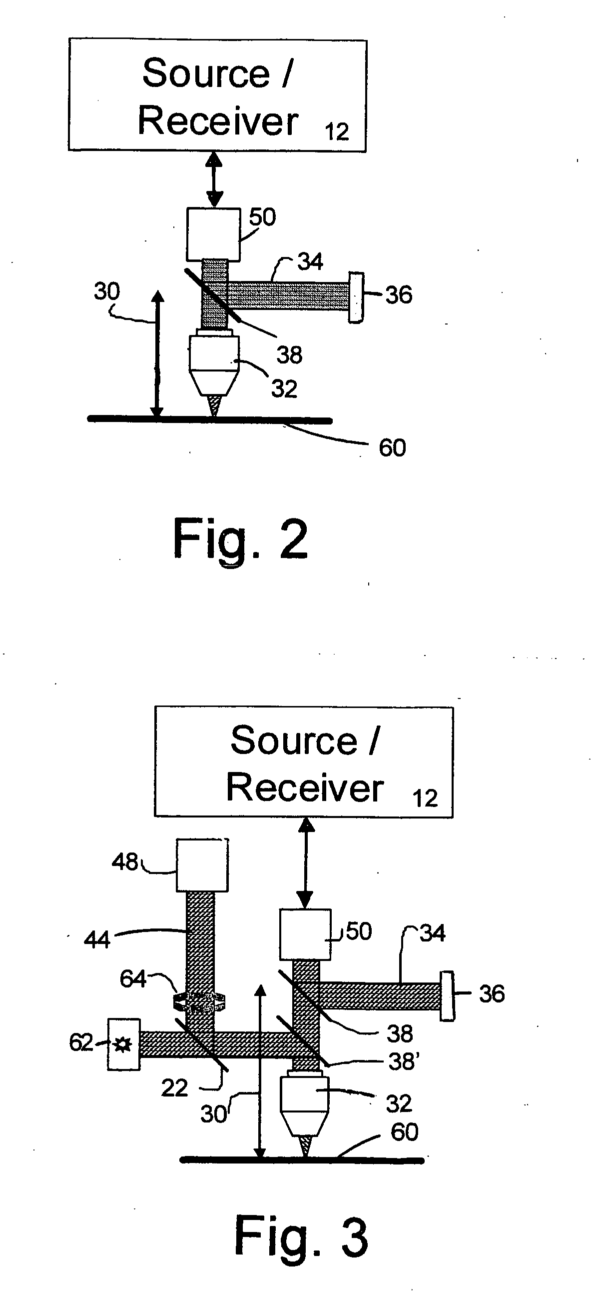
[0061]Several system embodiments are discussed below. They all have the common features of a broadband source, a measurement leg comprised of optics to illuminate ...


PUM


Abstract

A device (10) and methods for simultaneously measuring the thickness of individual wafer layers, the depth of etched features on a wafer, and the three-dimensional profile of a wafer. The structure of the device (10) is comprised of a source/receiver section (12) having a broadband source (14), a receiver (16) and a signal processing section (20). An interferometer (28) separates or combines measurement and reference light and has a measurement leg (30) and a reference leg (34), and a reference mirror (36). The device (10) analyzes a received spectrum which is comprised of a measurement of intensity versus wavelength. There are two measurement methods disclosed: the first method is utilized for taking a single measurement and the second method is utilized for multiple measurements.

Description

TECHNICAL FIELD[0001]The invention generally pertains to optical measuring devices and methods, and more particularly to a device and methods for simultaneously measuring three aspects of a test object such as a wafer.BACKGROUND ART[0002]There is a relentless effort to make electronics and memory circuits smaller, which continues to drive semiconductor manufacturers. The industry is currently developing 3D integrated circuits (3DICs), which requires physically stacking integrated circuit chips and using Through Silicon Vias (TSV) filled with a conductor to electrically connect the chips. The 3DICs create new possibilities for miniaturization and circuit architectures. There are a variety of techniques and technologies required to facilitate 3DICs and the construction of TSVs. A hole utilized for a TSV is typically 5 to 100 microns in diameter and typically 50 to 500 microns deep. These etched features, and others such as trenches, are called High Aspect Ratio features because they h...

Claims


Application Information

Patent Timeline
IPC IPC(8): G01B9/02
CPCG01B9/02004G01B9/0209G01B11/06G01B2210/56G01B11/22G01B11/2441G01B11/306G01B11/0675
Inventor MARX, DAVID S.GRANT, DAVID L.
Owner ONTO INNOVATION INC
Why Eureka
Try Eureka