Semiconductor element, memory circuit, integrated circuit, and driving method of the integrated circuit

a technology of semiconductor elements and driving methods, applied in semiconductor devices, digital storage, instruments, etc., can solve the problems of increasing circuit area, difficult to cope with a further increase in circuit scale by miniaturizing a single element, and low current generation in the region of oxide semiconductor layers where a channel is not formed, so as to reduce the area of the circuit, suppress the increase in circuit scale, and reduce the effect of circuit area

Inactive Publication Date: 2012-10-18
SEMICON ENERGY LAB CO LTD
View PDF0 Cites 6 Cited by
  • Summary
  • Abstract
  • Description
  • Claims
  • Application Information

AI Technical Summary

Benefits of technology

[0013]In a semiconductor element of one embodiment of the present invention, two different electrical switches are formed using a single oxide semiconductor layer. Therefore, the circuit area can be reduced as compared to the case where two electrical switches are separately provided (for example, the case where two transistors are separately provided). That is, a circuit is formed using the semiconductor element, whereby, an increase in the circuit area due to an increase in circuit scale can be suppressed.

Problems solved by technology

However, a mere increase in circuit scale causes an increase in the circuit area.
However, the research and development have been conducted for several decades and thus it is difficult to cope with a further increase in circuit scale by miniaturization of a single element.
Therefore, a current generated in a region of the oxide semiconductor layer where a channel is not formed can be extremely low.

Method used


Image

  • Semiconductor element, memory circuit, integrated circuit, and driving method of the integrated circuit
  • Semiconductor element, memory circuit, integrated circuit, and driving method of the integrated circuit
  • Semiconductor element, memory circuit, integrated circuit, and driving method of the integrated circuit

Examples


Embodiment Construction

[0022]Hereinafter, embodiments of the present invention will be described in detail with reference to the accompanying drawings. Note that the present invention is not limited to the description below, and it is easily understood by those skilled in the art that a variety of changes and modifications can be made without departing from the spirit and scope of the present invention. Therefore, the present invention should not be construed as being limited to the following description of the embodiments.

[0023]First, a semiconductor element according to one embodiment of the present invention will be described with reference to FIGS. 1A to 1C and FIGS. 2A to 2C.

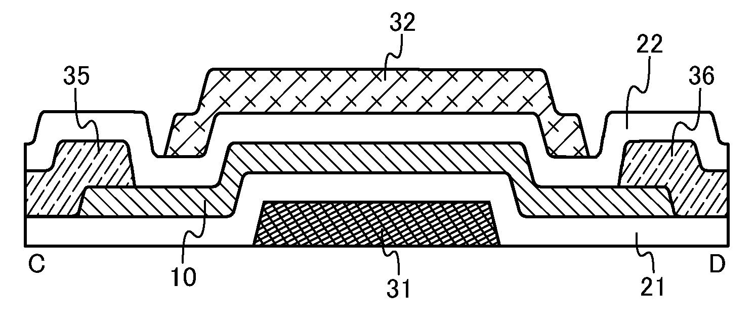
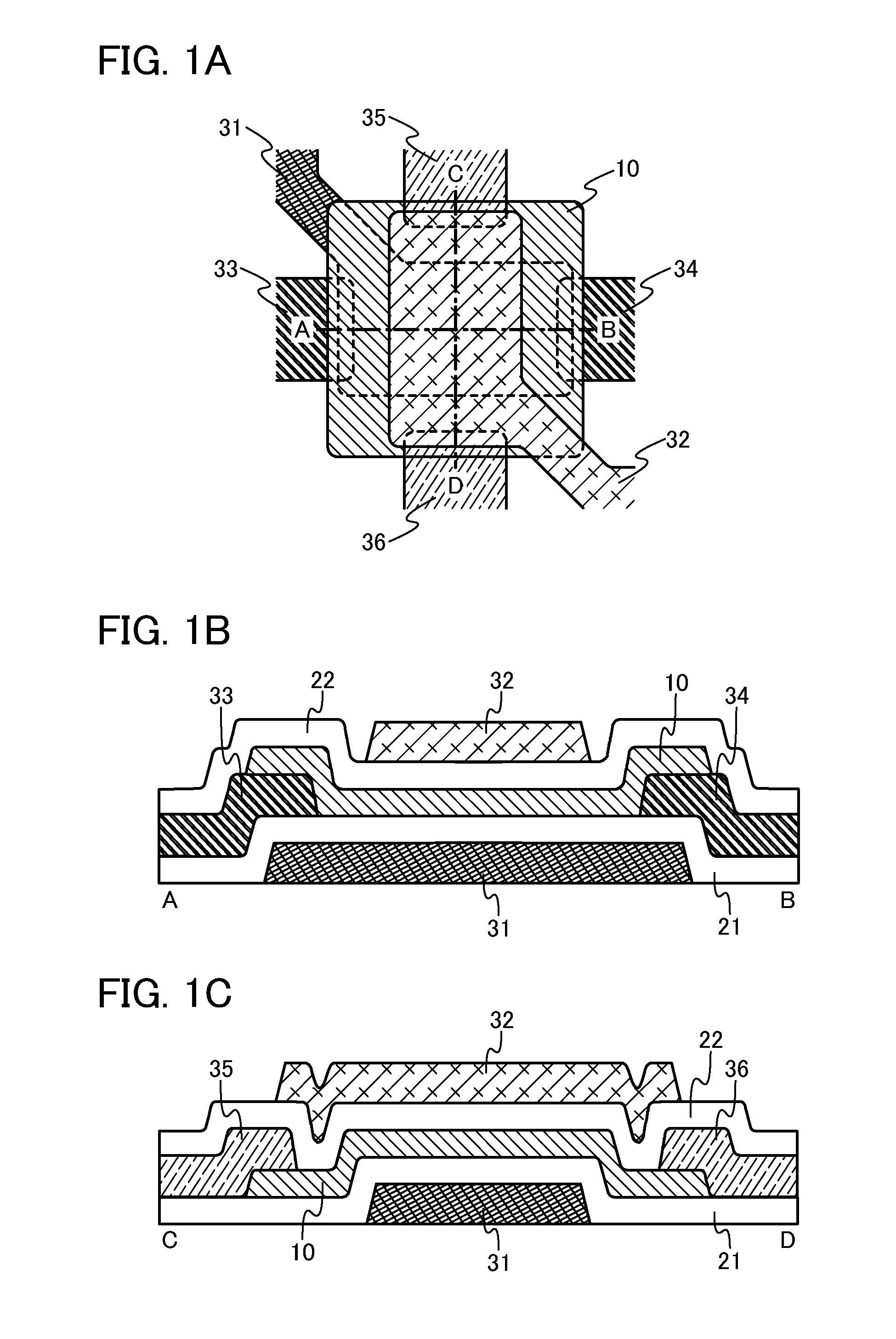
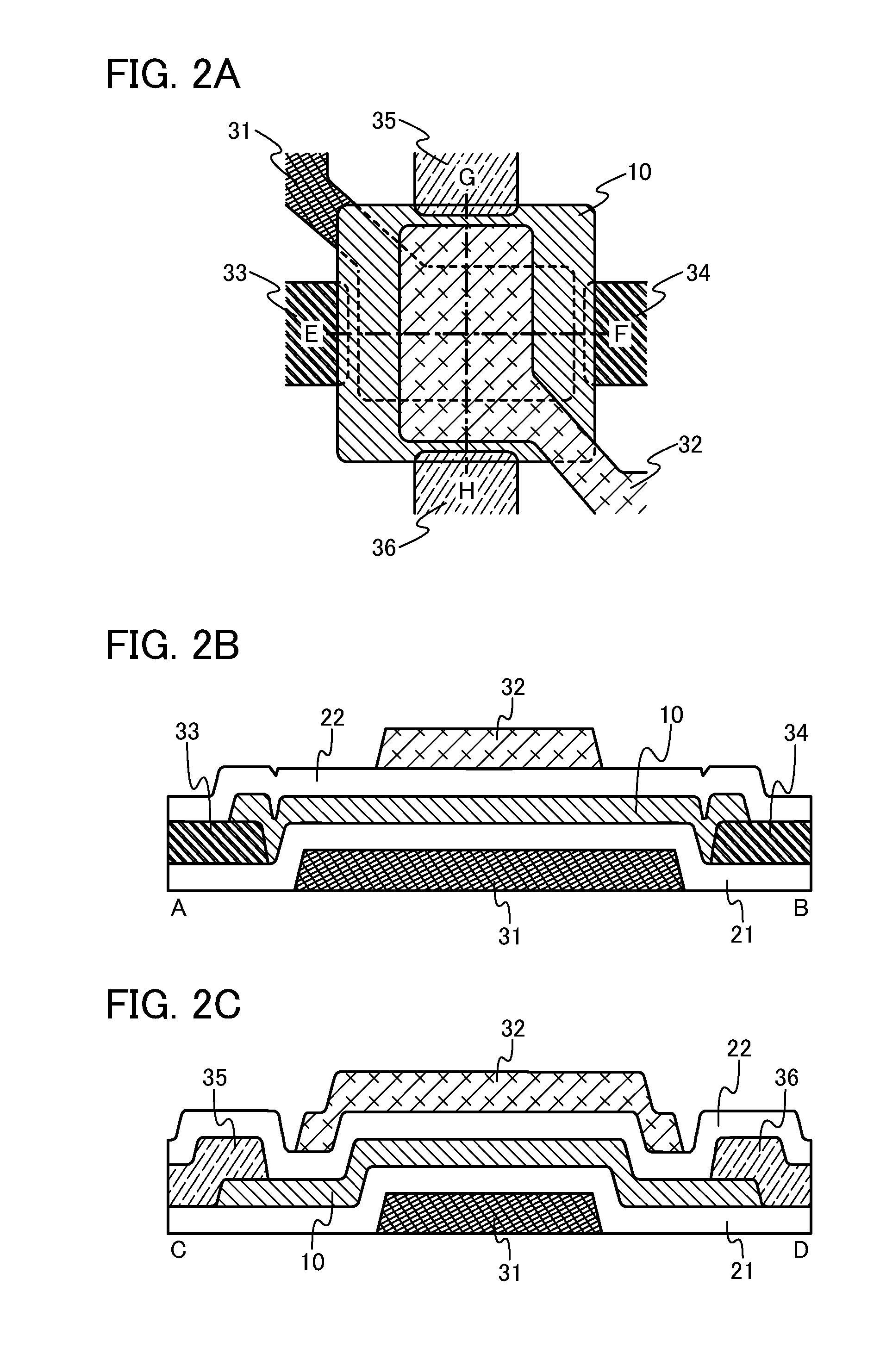
[0024]FIGS. 1A to 1C illustrate a structural example of a semiconductor element according to one embodiment of the present invention. FIG. 1A is a top view of the semiconductor element, and FIGS. 1B and 1C are a cross-sectional view along line A-B in FIG. 1A and a cross-sectional view along line C-D in FIG. 1A, respectively.

[0025...


PUM


Abstract

A novel semiconductor element contributing to an increase in circuit scale is provided. In the semiconductor element, two different electrical switches are formed using a single oxide semiconductor layer. For example, in the semiconductor element, formation of a channel (a current path) in the vicinity of a bottom surface (a first surface) of the oxide semiconductor layer and formation of a channel in the vicinity of a top surface (a second surface) of the oxide semiconductor layer are independently controlled. Therefore, the circuit area can be reduced as compared to the case two electrical switches are separately provided (for example, the case where two transistors are separately provided). That is, a circuit is formed using the semiconductor element, whereby an increase in the circuit area due to an increase in circuit scale can be suppressed.

Description

BACKGROUND OF THE INVENTION[0001]1. Field of the Invention[0002]The present invention generally relates to a semiconductor device. Specifically, the present invention relates to a semiconductor element having a function of an electrical switch. Further, the present invention relates to a memory circuit including the semiconductor element and an integrated circuit including the memory circuit. Furthermore, the present invention relates to a driving method of the integrated circuit.[0003]2. Description of the Related Art[0004]In recent years, a metal oxide having semiconductor characteristics, which is 4called an oxide semiconductor exhibiting high mobility and uniform element characteristics, has attracted attention as a material of a transistor. Metal oxides are used for a variety of applications. For example, indium oxide is used as a material of a pixel electrode in a liquid crystal display device. Examples of such metal oxides showing semiconductor characteristics include tungste...

Claims


Application Information

Patent Timeline
Patent Type & Authority Applications(United States)
IPC IPC(8): G11C7/10H01L29/786
CPCG11C11/40G11C13/0007H01L21/84H01L29/7869H01L27/1156H01L27/1203H01L27/10873H10B12/05H10B41/70
Inventor SAKATA, JUNICHIRO
Owner SEMICON ENERGY LAB CO LTD
Why Eureka
Try Eureka