Check patentability & draft patents in minutes with Patsnap Eureka AI!

Substrate for in-cell type touch sensor liquid crystal display device and method of fabricating the same

a liquid crystal display device and in-cell technology, applied in static indicating devices, instruments, optics, etc., can solve the problems of the disadvantage of viewing angle of the lcd device driven using the vertical electric field, and the deterioration of the contact property of the drain electrode and the data pad

Active Publication Date: 2012-10-25
LG DISPLAY CO LTD
View PDF5 Cites 102 Cited by
  • Summary
  • Abstract
  • Description
  • Claims
  • Application Information

AI Technical Summary

Benefits of technology

[0014]An array substrate for an in-cell type touch sensor liquid crystal display device includes: a substrate including a plurality of touch blocks each including a plurality of pixel regions; a gate line and a data line on the substrate, the gate line and the data line crossing each other with an interlayer insulating layer interposed therebetween to define each of the plurality of pixel regions; a thin film transistor connected to the gate line and the data line; a first passivation layer on the thin film transistor, the first passivation layer having a first drain contact hole exposing a drain electrode of the thin film transistor; a common electrode on the first passivation layer in each of the plurality of touch blocks; an etching preventing pattern covering the d...

Problems solved by technology

However, the LCD device driven using the vertical electric field has a disadvantage in viewing angle.
The exposed drain electrode and the data pad may be deteriorated due to an etching solution for a common electrode of a transparent material or a solution for a sensing line of a metallic material on the first passivation layer.
As a result, a contact property of the drain electrode and the data pad is deteriorated.

Method used


Image

  • Substrate for in-cell type touch sensor liquid crystal display device and method of fabricating the same
  • Substrate for in-cell type touch sensor liquid crystal display device and method of fabricating the same
  • Substrate for in-cell type touch sensor liquid crystal display device and method of fabricating the same

Examples


Embodiment Construction

[0026]Reference will now be made in detail to the preferred embodiments, examples of which are illustrated in the accompanying drawings.

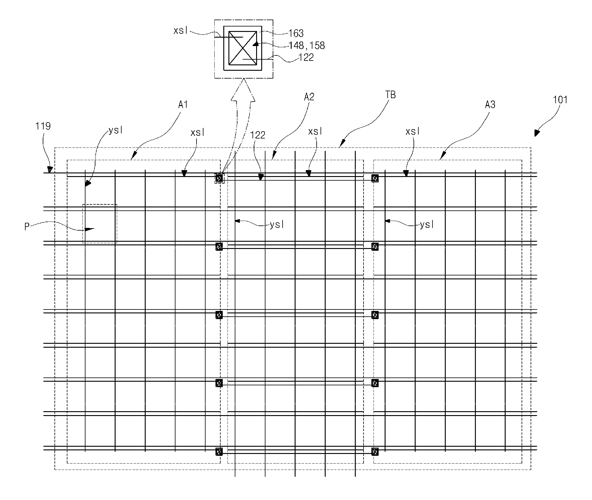
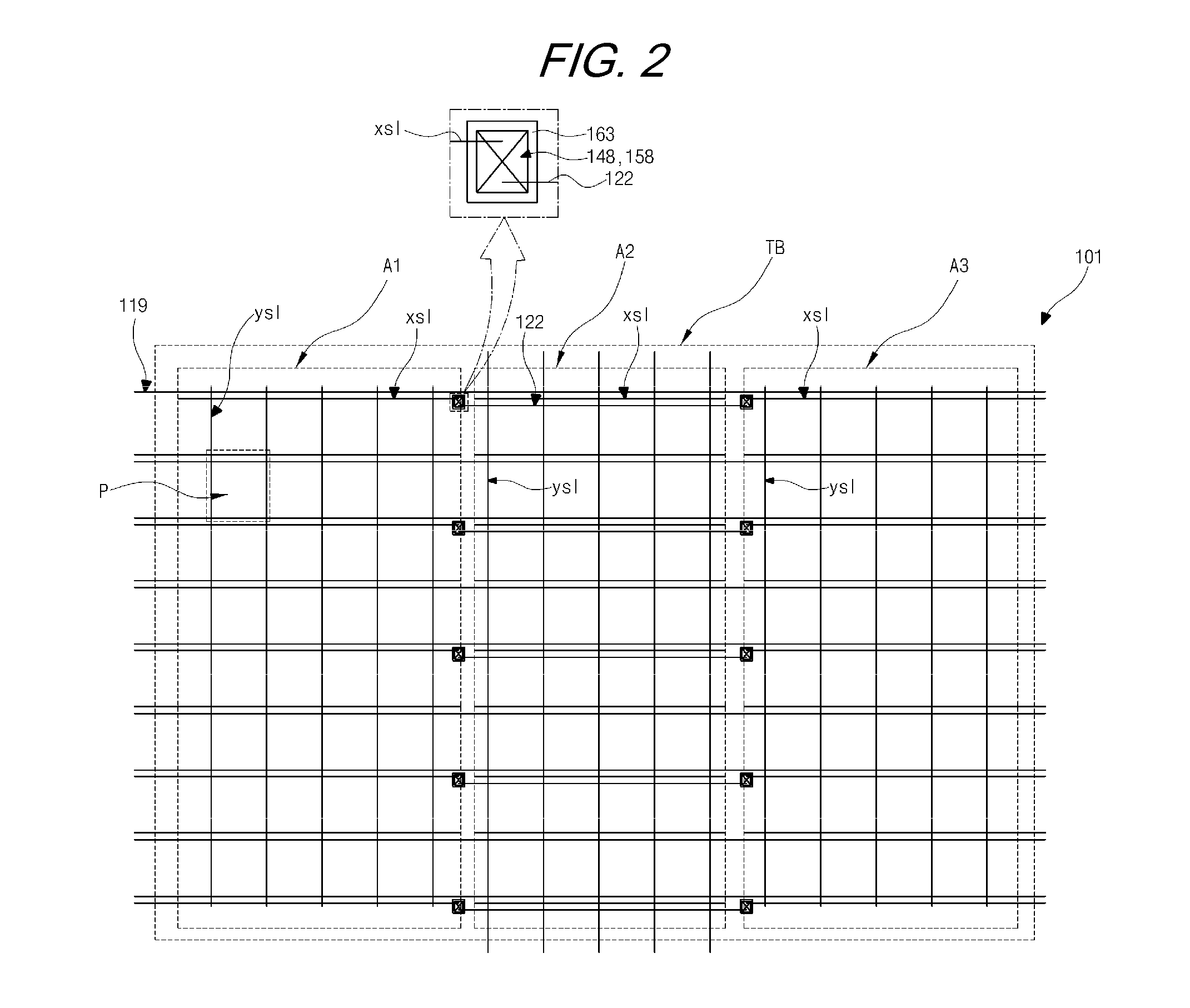
[0027]FIG. 2 is a plan view showing a touch block of an array substrate for an in-cell type touch sensor liquid crystal display device according to an embodiment of the present invention, and FIG. 3 is a cross-sectional view showing a pixel region of an array substrate for an in-cell type touch sensor liquid crystal display device according to an embodiment of the present invention. In addition, FIG. 4 is a cross-sectional view showing a pad area of an array substrate for an in-cell type touch sensor liquid crystal display device according to an embodiment of the present invention, and FIG. 5 is a cross-sectional view showing an end portion of a touch block of an array substrate for an in-cell type touch sensor liquid crystal display device according to an embodiment of the present invention.

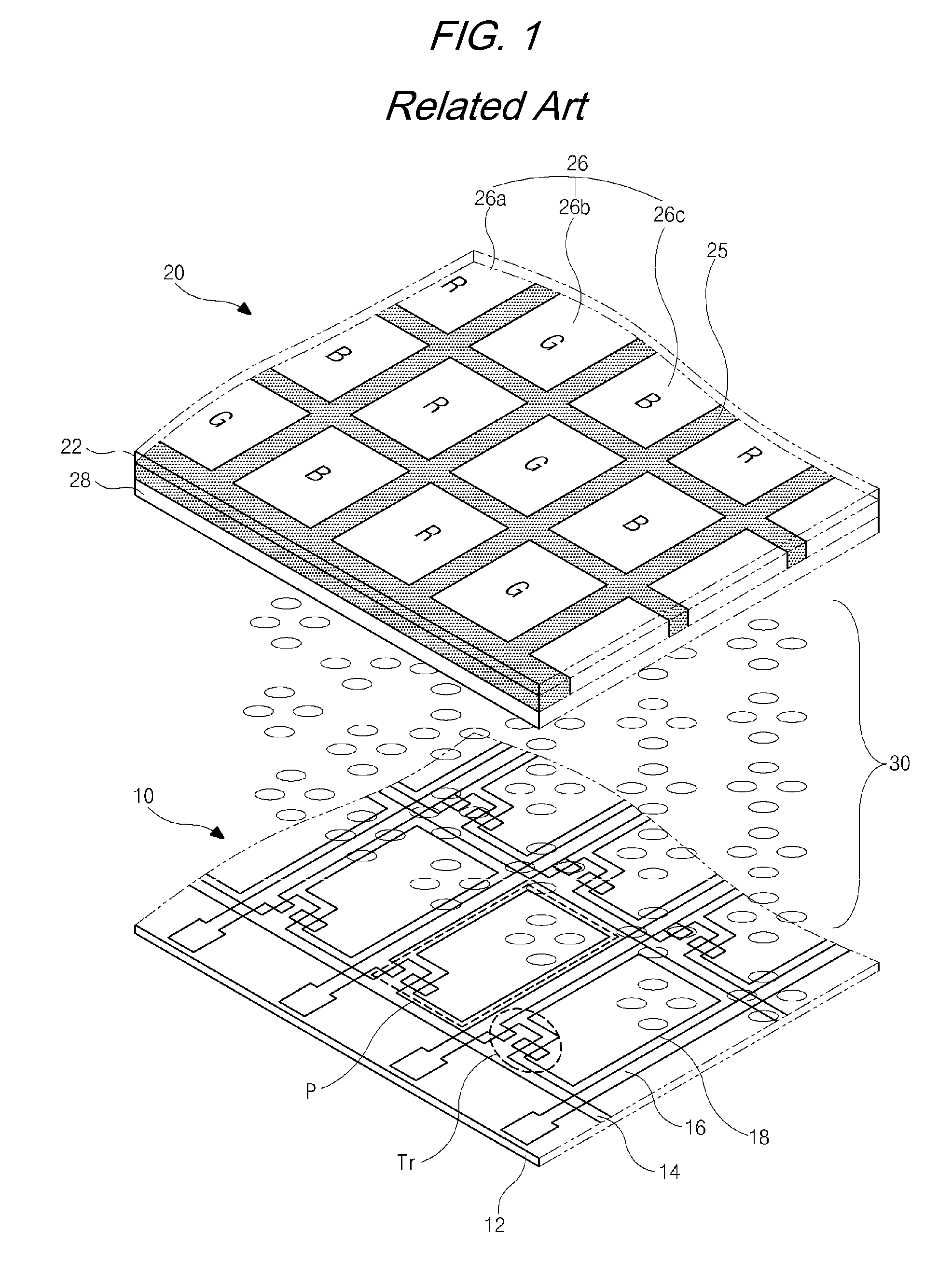
[0028]In FIGS. 2 to 5, an array substrate 101 for an in-ce...


PUM


Abstract

An array substrate for an in-cell type touch sensor liquid crystal display device includes: a substrate; a gate line and a data line on the substrate; a thin film transistor connected to the gate line and the data line; a first passivation layer on the thin film transistor; a common electrode on the first passivation layer; an etching preventing pattern covering the drain contact hole; an x sensing line and a y sensing line on the common electrode; a second passivation layer on the x sensing line and the y sensing line; and a pixel electrode on the second passivation layer.

Description

[0001]The present application claims the benefit of Korean Patent Application No. 10-2011-0037243 filed in Korea on Apr. 21, 2011, which is hereby incorporated by reference in its entirety.BACKGROUND[0002]1. Field of the Disclosure[0003]The present disclosure relates to a liquid crystal display device, and more particularly, to a substrate for an in-cell type touch sensor liquid crystal display device including where an electrical shortage between metal patterns in a contact hole is prevented and a method of fabricating the substrate.[0004]2. Discussion of the Related Art[0005]Recently, a liquid crystal display (LCD) device has been in the spotlight as a next generation display device having high value added because of its low power consumption and good portability. An active matrix liquid crystal display (AM-LCD) device, which includes thin film transistors as a switching device for a plurality of pixels, has been widely used due to its high resolution and superiority in displaying...

Claims


Application Information

Patent Timeline
IPC IPC(8): G09G3/36H01L31/12G06F3/041
CPCG06F3/0412G06F3/044G02F2001/134372G02F1/136227G02F1/13338G06F3/0443G06F3/0446G02F1/134372G06F2203/04103G02F1/136286G02F1/1368G06F3/047G02F1/136295H01L27/1274
Inventor KIM, MIN-SULEE, MYEONG-SIK
Owner LG DISPLAY CO LTD
Features
  • R&D
  • Intellectual Property
  • Life Sciences
  • Materials
  • Tech Scout
  • Unparalleled Data Quality
  • Higher Quality Content
  • 60% Fewer Hallucinations
Learn More