Image formation apparatus

a technology of image formation and apparatus, which is applied in the direction of printing, other printing apparatus, etc., can solve the problems of increasing the cost due to an increase of the number of parts, reducing the accuracy of the dot formation, etc., and achieve the effect of simple configuration

Inactive Publication Date: 2012-10-25
SEIKO EPSON CORP
View PDF5 Cites 0 Cited by
  • Summary
  • Abstract
  • Description
  • Claims
  • Application Information

AI Technical Summary

Benefits of technology

[0007]An advantage of some aspects of the invention is to provide an image formation apparatus configured to make it possible to measure t

Problems solved by technology

An overheated condition of a transistor for generating driving voltage pulses that are applied to a dot formation element leads to shape variations of the pulses; thereby causing accuracy of

Method used


Image

  • Image formation apparatus
  • Image formation apparatus
  • Image formation apparatus

Examples


first embodiment

1. First Embodiment

1-1. Configuration

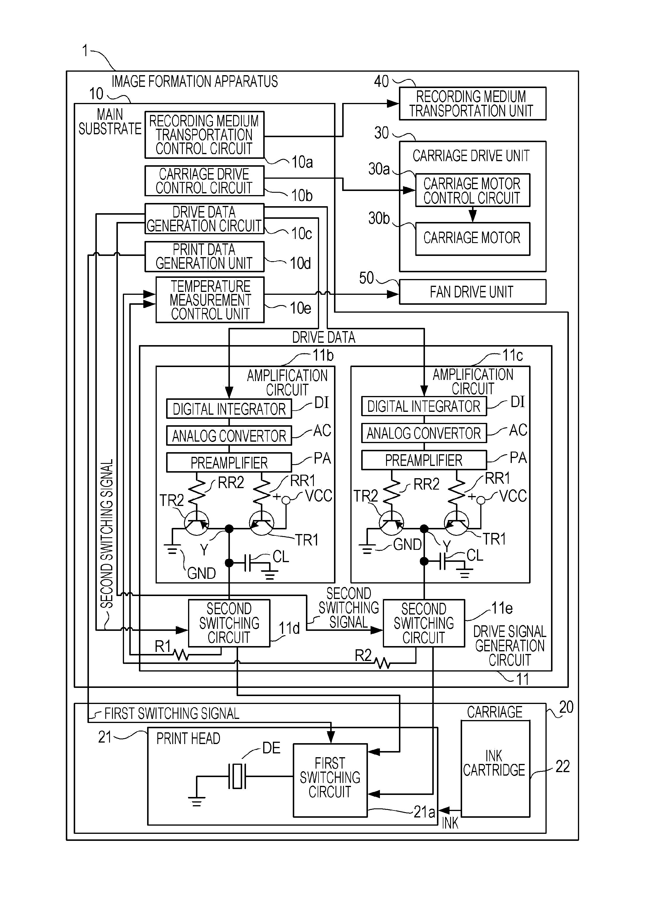
[0024]FIG. 1 is a block diagram illustrating an image formation apparatus 1 according to an embodiment of the invention. The image formation apparatus 1 is a serial ink jet printer which forms print images on a recording medium by reciprocating a print head thereof in the main scanning direction. The image formation apparatus 1 includes a main substrate 10, a carriage 20, a carriage drive unit 30, a recording medium transportation unit 40 and a fan drive unit 50. The main substrate 10 is a substrate on which a CPU, ROM modules, RAM modules, ASICs and the like are mounted, and includes a recording medium transportation control circuit 10a, a carriage drive control circuit 10b, a drive data generation circuit 10c, a print data generation section 10d, a temperature measurement control unit 10e and a drive signal generation circuit 11. The drive data generation circuit 10c and the drive signal generation circuit 11 correspond to a voltage signal gene...


PUM


Abstract

An image formation apparatus includes a dot formation element; a voltage signal generation circuit configured to generate a voltage signal by using an amplification circuit including a transistor, the voltage signal including a plurality of driving voltage pulses each thereof driving the dot formation element, and at least one temperature measurement voltage portion each thereof being provided between two successive ones of the driving voltage pulses; a temperature measurement control unit configured to measure a temperature of the transistor on the basis of the voltage signal; and a switch circuit configured to output the voltage signal to the dot formation element during a period when the transistor amplifies a signal corresponding to each of the driving voltage pulses, and output the voltage signal to the temperature measurement control unit during a period when the transistor amplifies a signal corresponding to each of the at least one temperature measurement voltage portion.

Description

[0001]The entire disclosure of Japanese Patent Application No. 2011-094779, filed on Apr. 21, 2011 is expressly incorporated herein by reference.BACKGROUND[0002]1. Technical Field[0003]The present invention relates to an image formation apparatus having a function of measuring the temperature of a transistor for generating driving voltage pulses applied to a dot formation element thereof.[0004]2. Related Art[0005]Various methods for measuring the junction temperature of a transistor have been well known to those skilled in the art (for example, refer to JP-A-64-16972). Further, it has been well known to those skilled in the art that a transistor can be used as a means for measuring temperature (for example, refer to JP-A-2004-150897 and JP-A-2001-116624).[0006]An overheated condition of a transistor for generating driving voltage pulses that are applied to a dot formation element leads to shape variations of the pulses; thereby causing accuracy of the dot formation to be reduced. Th...

Claims


Application Information

Patent Timeline
IPC IPC(8): B41J29/38
CPCB41J2/04515B41J2/04541B41J29/38B41J2/04581B41J2/04588B41J2/04563
Inventor TSUYUKI, MASAHIKO
Owner SEIKO EPSON CORP
Why Eureka
Try Eureka