Semiconductor device and method for manufacturing the same

a semiconductor and transistor technology, applied in semiconductor devices, instruments, electrical equipment, etc., can solve the problems of significant signal delay due to resistance of wiring, low frequency characteristics (called “f characteristics”), and hinder the high speed operation of thin film transistors, etc., to achieve small parasitic capacitance, small photoelectric current, and high on-off ratio

Active Publication Date: 2012-11-01
SEMICON ENERGY LAB CO LTD
View PDF6 Cites 107 Cited by
  • Summary
  • Abstract
  • Description
  • Claims
  • Application Information

AI Technical Summary

Benefits of technology

[0009]For a thin film transistor in which a channel formation region is formed using an oxide semiconductor film, high speed operation, a comparatively-easy manufacturing process, and sufficient reliability are required.

Problems solved by technology

In particular, when a display device with a large-area display is manufactured, a problem of signal delay due to resistance of a wiring significantly arises.
In addition, capacitance is formed in a portion where the source and drain electrodes and the oxide semiconductor film have a direct contact with each other, and there are risks that frequency characteristics (called “f characteristics”) decrease and high speed operation of the thin film transistor is hindered.

Method used


Image

  • Semiconductor device and method for manufacturing the same
  • Semiconductor device and method for manufacturing the same
  • Semiconductor device and method for manufacturing the same

Examples


embodiment 1

[0070]In this embodiment, a thin film transistor and a manufacturing process thereof will be described with reference to FIGS. 1A to 1D, FIGS. 2A and 2B, FIGS. 3A to 3G, and FIGS. 4A to 4D.

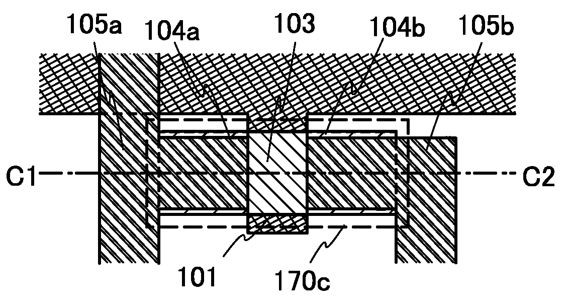
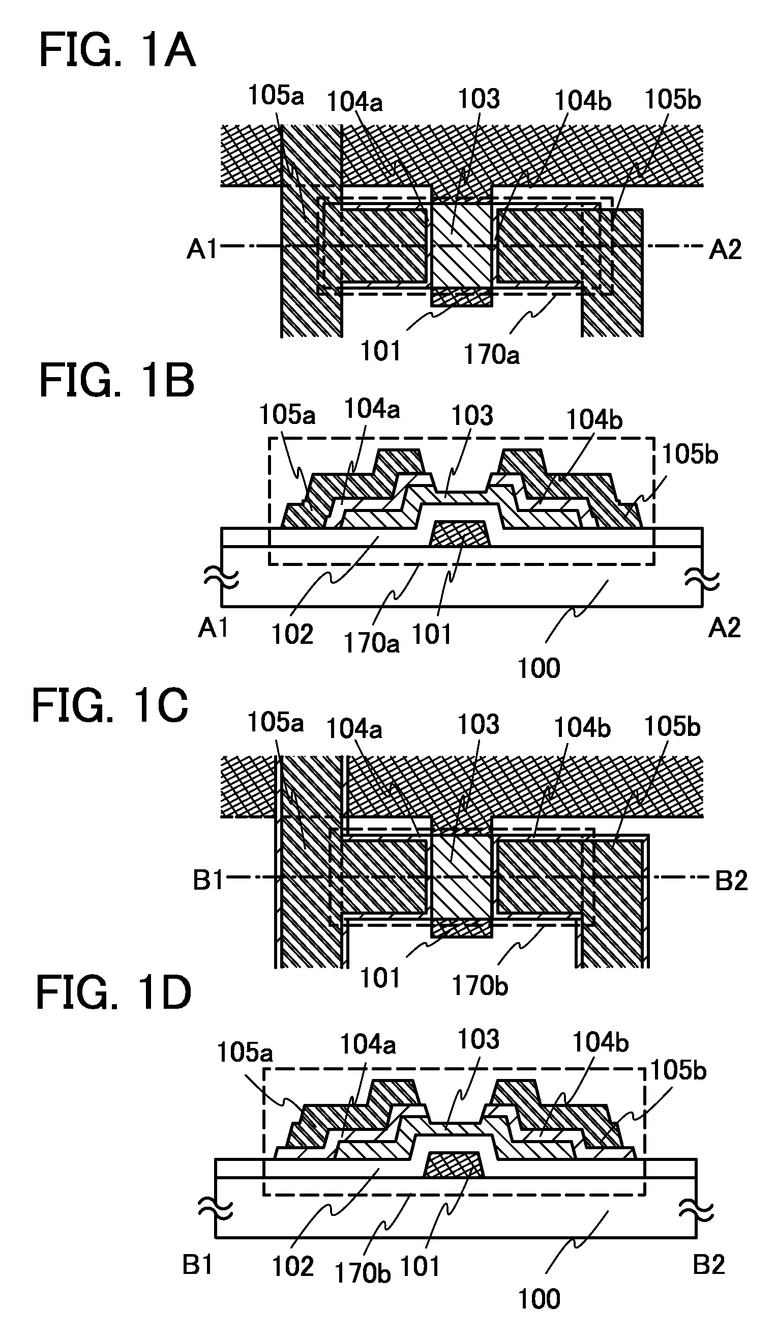
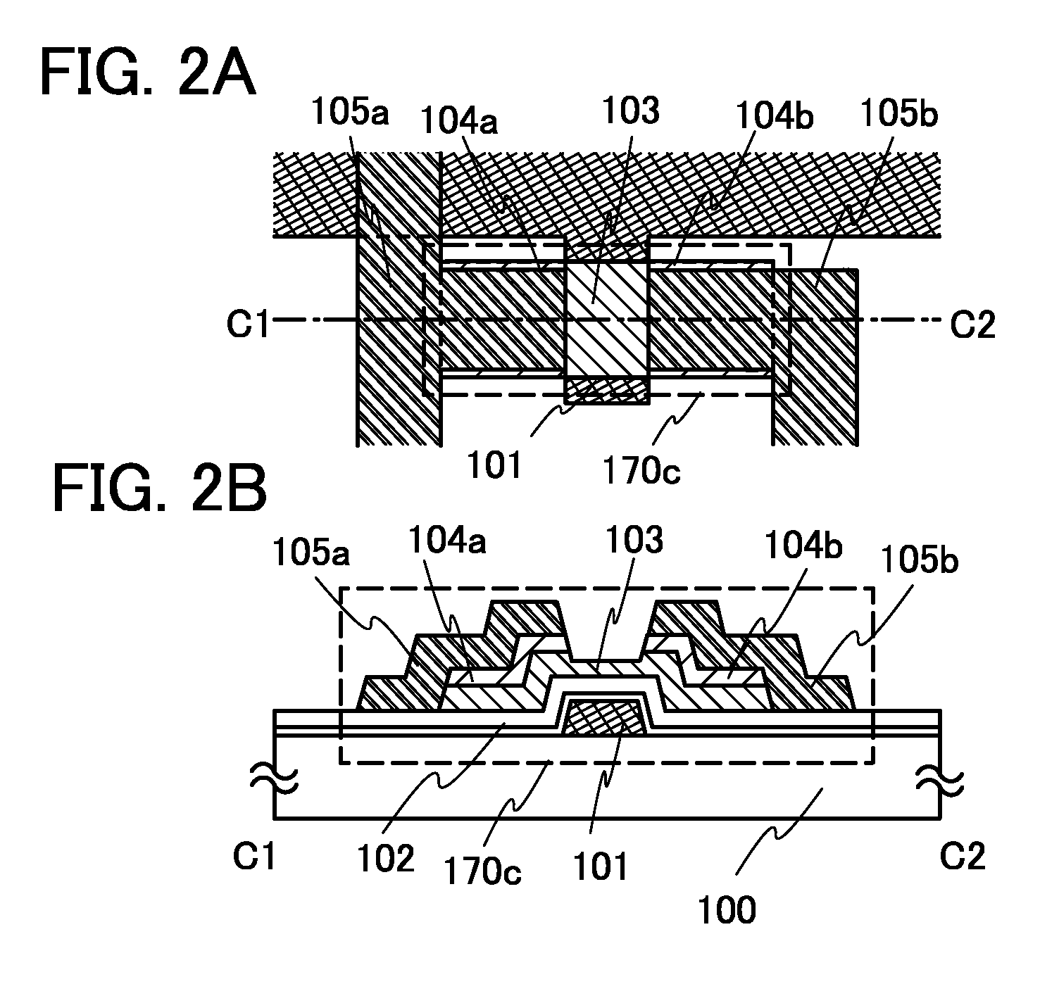
[0071]Thin film transistors 170a, 170b, and 170c each having a bottom gate structure of this embodiment are illustrated in FIGS. 1A to 1D and FIGS. 2A and 2B. FIG. 1A is a plan view and FIG. 1B is a cross-sectional view taken along a line A1-A2 of FIG. 1A. FIG. 1C is a plan view and FIG. 1D is a cross-sectional view taken along a line B1-B2 of FIG. 1C. FIG. 2A is a plan view and FIG. 2B is a cross-sectional view taken along a line C1-C2 of FIG. 2A.

[0072]In FIGS. 1A and 1B, over a substrate 100, the thin film transistor 170a which includes a gate electrode layer 101, a gate insulating layer 102, a semiconductor layer 103, n-type buffer layers 104a and 104b, and a source and drain electrode layers 105a and 105b is provided.

[0073]As the semiconductor layer 103, an oxide semiconductor film containing ...

embodiment 2

[0132]In this embodiment, an example of a thin film transistor having a multi-gate structure will be described. Accordingly, except the gate structure, the thin film transistor can be formed in a manner similar to Embodiment 1, and repetitive description of the same portions as or portions having functions similar to those in Embodiment 1 and manufacturing steps will be omitted.

[0133]In this embodiment, a thin film transistor included in a semiconductor device will be described with reference to FIGS. 5A and 5B, FIGS. 6A and 6B, and FIGS. 7A and 7B.

[0134]FIG. 5A is a plan view illustrating a thin film transistor 171a and FIG. 5B is a cross-sectional view of the thin film transistor 171a taken along a line E1-E2 of FIG. 5A.

[0135]As illustrated in FIGS. 5A and 5B, over a substrate 150, a thin film transistor 171a having a multi-gate structure, which includes gate electrode layers 151a and 151b, a gate insulating layer 152, semiconductor layers 153a and 153b, buffer layers 154a, 154b, ...

embodiment 4

[0156]In this embodiment, an example in which a shape of the thin film transistor and a manufacturing method of the thin film transistor are partly different from those of Embodiment 1. Except the shape, the thin film transistor can be formed in a manner similar to Embodiment 1; thus, repetitive description of the same portions as or portions having functions similar to those in Embodiment 1 and manufacturing steps will be omitted.

[0157]In this embodiment, a thin film transistor 174 used in a display device and manufacturing steps thereof will be described with reference to FIGS. 9A and 9B and FIGS. 10A to 10D. FIG. 9A is a plan view of the thin film transistor 174, FIG. 9B is a cross-sectional view thereof taken along a line D1-D2 of FIG. 9A, and FIGS. 10A to 10D are cross-sectional views illustrating manufacturing steps thereof taken along the line D1-D2.

[0158]As illustrated in FIGS. 9A and 9B, over the substrate 100, the thin film transistor 174 including the gate electrode layer...


PUM


Abstract

An embodiment is to include an inverted staggered (bottom gate structure) thin film transistor in which an oxide semiconductor film containing In, Ga, and Zn is used as a semiconductor layer and a buffer layer is provided between the semiconductor layer and a source and drain electrode layers. The buffer layer having higher carrier concentration than the semiconductor layer is provided intentionally between the source and drain electrode layers and the semiconductor layer, whereby an ohmic contact is formed.

Description

BACKGROUND OF THE INVENTION[0001]1. Field of the Invention[0002]The present invention relates to a semiconductor device which has a circuit including a thin film transistor (hereinafter, referred to as a TFT) in which a channel formation region is formed using an oxide semiconductor film and a manufacturing method thereof For example, the present invention relates to an electronic appliance in which an electro-optical device typified by a liquid crystal display panel or a light-emitting display device including an organic light-emitting element is mounted as its component.[0003]Note that the semiconductor device in this specification indicates all the devices which can operate by using semiconductor characteristics, and an electro-optical device, a semiconductor circuit, and an electronic appliance are all included in the semiconductor devices.[0004]2. Description of the Related Art[0005]In recent years, active matrix display devices (such as liquid crystal display devices, light-em...

Claims


Application Information

Patent Timeline
Patent Type & Authority Applications(United States)
IPC IPC(8): H01L29/12
CPCH01L29/7869H01L27/1225H01L29/78645H01L29/45G02F1/1368G02F1/136227G02F1/1339G02F1/13606G02F2202/10H10K59/1213G02F1/133345G02F1/133528G02F1/134336G02F1/13439G02F1/136286G02F2201/123G09G3/3674G09G2310/0286H01L29/247H01L29/66969H01L29/78618H01L29/78648H01L29/78693H01L29/78696
Inventor YAMAZAKI, SHUNPEIMIYAIRI, HIDEKAZUMIYANAGA, AKIHARUAKIMOTO, KENGOSHIRAISHI, KOJIRO
Owner SEMICON ENERGY LAB CO LTD
Why Eureka
Try Eureka