Semiconductor device and method for manufacturing the same

a semiconductor and semiconductor technology, applied in the field of semiconductor devices, can solve the problems of significant signal delay due to wiring resistance, hinder the high-speed operation of thin-film transistors, etc., and achieve the effects of low parasitic capacitance, low parasitic capacitance, and low cos

Active Publication Date: 2010-02-11
SEMICON ENERGY LAB CO LTD
View PDF8 Cites 39 Cited by
  • Summary
  • Abstract
  • Description
  • Claims
  • Application Information

AI Technical Summary

Benefits of technology

[0039]According to the present invention, a thin film transistor having a small amount of photocurrent, low parasitic capacitance, a high on-off ratio, and good dynamic characteristics can be manufactured. Accordingly, a semiconductor device including a thin film transistor having high electrical properties and high reliability can be provided.

Problems solved by technology

In particular, in the case of manufacturing a display device having a large display area, the problem of signal delay due to wiring resistance becomes significant.
In addition, capacitance is formed in a portion where the oxide semiconductor film and the source and drain electrodes are directly in contact with each other, and frequency characteristics (referred to as F characteristics) are lowered, which might hinder high-speed operation of the thin film transistor.

Method used


Image

  • Semiconductor device and method for manufacturing the same
  • Semiconductor device and method for manufacturing the same
  • Semiconductor device and method for manufacturing the same

Examples


embodiment 1

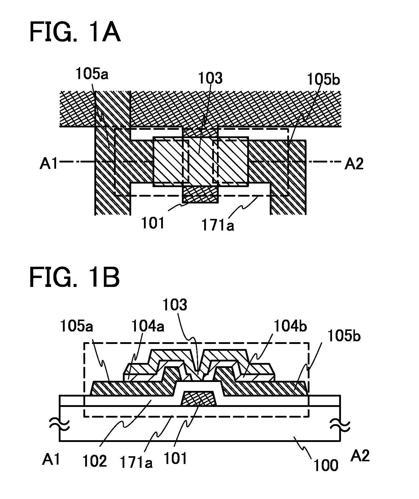
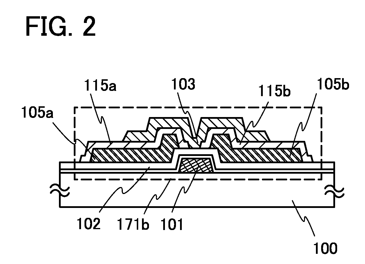
[0067]In this embodiment, a thin film transistor and a manufacturing process thereof will be described with reference to FIGS. 1A and 1B and FIG. 2.

[0068]Thin film transistors 171a and 171b of this embodiment, each having a kind of bottom gate structure (also referred to as a bottom contact structure), are illustrated in FIGS. 1A and 1B and FIG. 2. FIG. 1A is a plan view and FIG. 1B is a cross-sectional view taken along line A1-A2 of FIG. 1A.

[0069]In FIGS. 1A and 1B, the thin film transistor 171a that includes a gate electrode layer 101, a gate insulating layer 102, a source and drain electrode layers 105a and 105b, n-type buffer layers 104a and 104b, and a semiconductor layer 103 is provided over a substrate 100.

[0070]As the semiconductor layer 103, an oxide semiconductor film containing In, Ga, and Zn is used. The buffer layers 104a and 104b having higher carrier concentration than the semiconductor layer 103 are intentionally provided between the source and drain electrode layers...

embodiment 2

[0110]In this embodiment, an example of a thin film transistor having a multi-gate structure, which is one embodiment of the present invention will be described. Accordingly, except the gate electrode layer, the thin film transistor can be formed in a manner similar to Embodiment 1, and repetitive description of the same portions or portions having functions similar to those in Embodiment 1 and manufacturing steps thereof will be omitted.

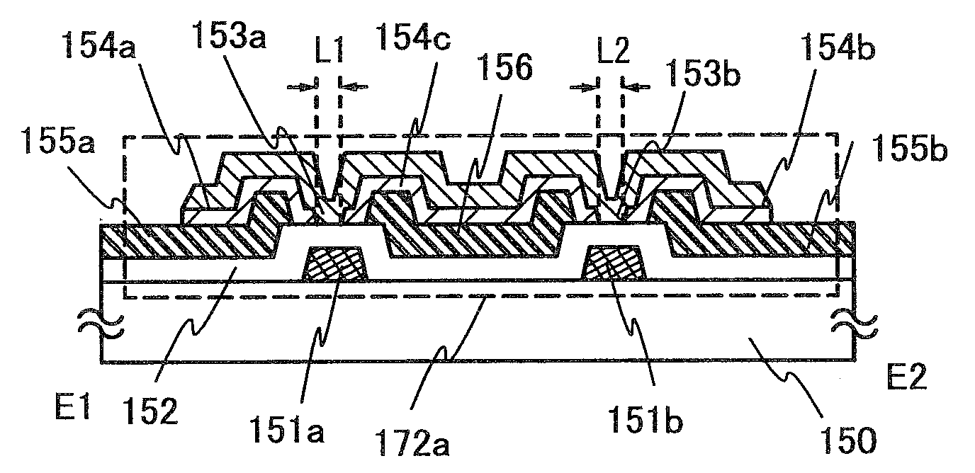
[0111]In this embodiment, a thin film transistor included in a semiconductor device will be described with reference to FIGS. 4A and 4B and FIGS. 5A and 5B.

[0112]FIG. 4A is a plan view illustrating a thin film transistor 172a and FIG. 4B is a cross-sectional view of the thin film transistor 172a taken along line E1-E2 of FIG. 4A.

[0113]As illustrated in FIGS. 4A and 4B, the thin film transistor 172a having a multi-gate structure, which includes gate electrode layers 151a and 151b, a gate insulating layer 152, a source and drain electrode layers 155a ...

embodiment 3

[0122]In this embodiment, an example of a display device which is one example of a semiconductor device of one embodiment of the present invention will be described. In the display device, at least a part of a driver circuit and a thin film transistor to be disposed in a pixel portion are formed over one substrate.

[0123]The thin film transistor to be disposed in the pixel portion is formed according to Embodiment 1 or 2. Further, the thin film transistor described in Embodiment 1 or 2 is an n-channel TFT, and thus a part of a driver circuit that can include an n-channel TFT among driver circuits is formed over the same substrate as the thin film transistor of the pixel portion.

[0124]FIG. 6A is an example of a block diagram of an active matrix liquid crystal display device which is an example of a semiconductor device of one embodiment of the present invention. The display device illustrated in FIG. 6A includes, over a substrate 5300, a pixel portion 5301 including a plurality of pix...


PUM


Abstract

One of the objects of the present invention is to provide a thin film transistor using an oxide semiconductor film containing indium (In), gallium (Ga), and zinc (Zn), in which the contact resistance between the oxide semiconductor layer and a source and drain electrodes is reduced, and to provide a method for manufacturing the thin film transistor. An ohmic contact is formed by intentionally providing a buffer layer having a higher carrier concentration than the IGZO semiconductor layer between the IGZO semiconductor layer and the source and drain electrode layers.

Description

BACKGROUND OF THE INVENTION[0001]1. Field of the Invention[0002]The present invention relates to a semiconductor device having a circuit including a thin film transistor (hereinafter, referred to as a TFT) in which a channel formation region is formed using an oxide semiconductor film, and a method for manufacturing the same. For example, the present invention relates to an electronic appliance in which an electro-optical device typified by a liquid crystal display panel or a light-emitting display device including an organic light-emitting element is mounted as its component.[0003]Note that the semiconductor device in this specification indicates all the devices that can operate by using semiconductor characteristics, and an electro-optical device, a semiconductor circuit, and an electronic appliance are all included in the semiconductor devices.[0004]2. Description of the Related Art[0005]In recent years, active matrix display devices (such as liquid crystal display devices, light...

Claims


Application Information

Patent Timeline
Patent Type & Authority Applications(United States)
IPC IPC(8): H01L29/786H01L21/336
CPCH01L29/7869H01L29/78618H01L29/45
Inventor YAMAZAKI, SHUNPEIMIYAIRI, HIDEKAZUMIYANAGA, AKIHARUAKIMOTO, KENGOSHIRAISHI, KOJIRO
Owner SEMICON ENERGY LAB CO LTD
Why Eureka
Try Eureka