Circuit and method for sensing a differential capacitance

a differential capacitance and circuit technology, applied in the direction of resistance/reactance/impedence, measurement devices, instruments, etc., can solve the problems of deteriorating sensing performance, over-sampling operation under this configuration fails to effectively average charges and reduce noise, and the effect of reducing source noise and interferen

Inactive Publication Date: 2012-11-01
ELAN MICROELECTRONICS CORPORATION
View PDF2 Cites 15 Cited by
  • Summary
  • Abstract
  • Description
  • Claims
  • Application Information

AI Technical Summary

Benefits of technology

[0006]An objective of the present invention is to provide a circuit and a method for sensing differential capacitance capable of reducing RF interference and source noises.

Problems solved by technology

However, such an existing approach is not effective enough in noise reduction.
In other words, VOUT1 approximates Vn, so the over-sampling operation under this configuration fails to effectively average charges and reduce noises.
In addition, the amplifier stage 14 uses the operational amplifier to directly amplify the difference VCD between the corresponding output voltages VOUT1 and VOUT2, so the non-ideal effects of the operational amplifier (e.g. offsets, flicker noise and finite gain error) are output through the output terminal as well, making the sensing performance deteriorated.

Method used


Image

  • Circuit and method for sensing a differential capacitance
  • Circuit and method for sensing a differential capacitance
  • Circuit and method for sensing a differential capacitance

Examples


first embodiment

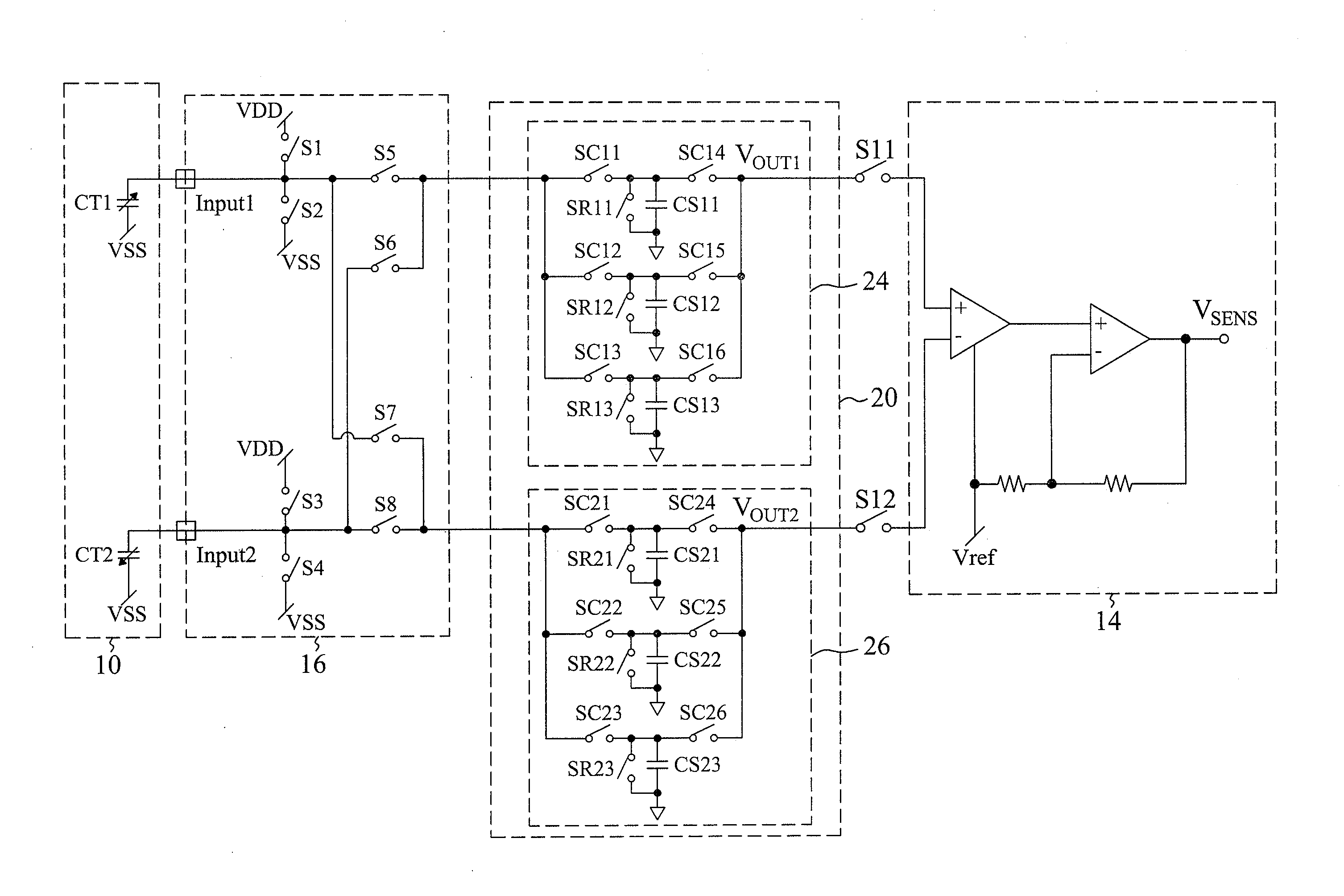
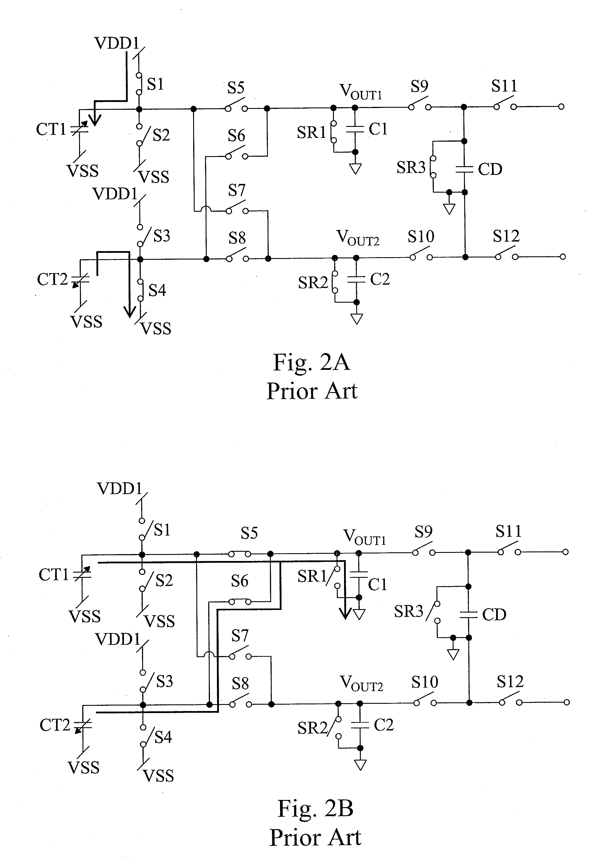
[0020]FIG. 3 is a circuit for sensing a differential capacitance according to the present invention. The circuit has a switching circuit 16, a charge-storing circuit 20 and an amplifier stage 22. The charge-storing circuit 20 includes a plurality of storing capacitors. During operation, it uses switches to make the charges sampled in each transfer round stored into a different storing capacitor, and then connects all the storing capacitors in parallel for outputting, so as to collect charge averages from both inputs and the noises. The switching circuit 16 is connected to capacitors CT1 and CT2 at sensing terminals Input1 and Input2, respectively. By switching switches S1-S8 in the switching circuit 16, the capacitors CT1 and CT2 are connected to a low-voltage source or a high-voltage source. Then the charges of the capacitors CT1 and CT2 are repeatedly transferred to the charge-storing circuit 20, as shown in FIGS. 2A-2D. For all the embodiments described herein, the power source V...

third embodiment

[0023]FIG. 6 is the circuit for sensing a differential capacitance according to the present invention. The circuit includes a switching circuit 16, a charge-storing circuit 30 and an amplifier stage 22. Similar to the embodiment of FIG. 3, the charge-storing circuit 30 also performs oversampling by using plural storing capacitors, but has three storing circuits 32, 34 and 36, wherein the principle of multiple storing capacitors is applied to the storing circuit 36 floated between the storing circuits 32 and 34. In this system, capacitors CS1 and CS2 in the storing circuits 32 and 34 sample capacitors CT1 and CT2, as shown in FIGS. 2A-2D. After the first transfer round, switches SCD1 and SCD2 are turned on, so as to store charges into the capacitor CD1. Then the capacitors CS1 and CS2 are reset, so that the charges similarly sampled in the second transfer round are stored into the capacitor CD2. Again, the capacitors CS1 and CS2 are reset to make the charges sampled in the third tran...


PUM


Abstract

A circuit and a method for sensing differential capacitance involve using plural storing capacitors to repeatedly sample charges of the differential capacitance in an over-sampling manner, and storing the charges sampled in different transfer rounds into different storing capacitors instead of repeatedly transferring charges for a single storing capacitor, so as to collect charge averages about both inputs and noises and in turn effectively reduce RF interference and source noises.

Description

FIELD OF THE INVENTION[0001]The present invention is related generally to a circuit for sensing differential capacitance and, more particularly, to a circuit and a method for sensing differential capacitance capable of reducing RF interference and source noises.BACKGROUND OF THE INVENTION[0002]Differential capacitance is also referred to as electrode capacitance, which is a difference between the capacitances formed at two electrodes. Sensors working thereupon have been developed and extensively used for sensing capacitive variations caused by physical factors, such as pressures, acceleration, linear displacement and rotational angles. While the circuit layouts may vary with practical sensing requirements, such sensors generally produce the sensing value according to the difference between the individual capacitances of two electrodes therein.[0003]U.S. Pat. No. 6,949,937 has proposed a sensing circuit as depicted in FIG. 1, which comprises a switched capacitor front-end 12 and an a...

Claims


Application Information

Patent Timeline
Patent Type & Authority Applications(United States)
IPC IPC(8): G01R27/26
CPCG01D5/24G01R17/02
Inventor YANG, CHAO-CHIPENG, SHIH-HOW
Owner ELAN MICROELECTRONICS CORPORATION
Why Eureka
Try Eureka