
Method of manufacturing array substrate, array substrate, method of manufacturing screen, and screen

Active Publication Date: 2012-11-01
SEIKO EPSON CORP
View PDF21 Cites 2 Cited by
  • Summary
  • Abstract
  • Description
  • Claims
  • Application Information

AI Technical Summary

Benefits of technology

[0009]According to such an array substrate, the plurality of convex portions, or concave portions which is formed in the array shape, and a groove are simultaneously transferred to and formed on the substrate as the array substrate, by the mold member having the shape of the convex portions, or concave portions which is formed on the substrate, and the groove. In addition, the outer edge portion may be easily cut out by setting the depth of the transferred groove to be less than that of the substrate, when tearing up the substrate, and the outer edge portion which is not necessary as the array substrate, on the basis of the groove which is transferred to the substrate. Accordingly, the gap between the edge of a region of the array substrate where the convex portion or the concave portion is formed and the edge of the array substrate becomes constant, and it is possible to realize an array substrate with high external dimension precision.Application Example 2
[0015]According to such a screen, the convex portion, or the concave portion in which the reflective film which causes the projection light to be reflected is formed, and the groove used for cutting out the outer edge portion which is not necessary as the screen are simultaneously formed by pressing and transferring the mold member which includes the shapes of the convex portion, or the concave portion, and the groove which are formed on the substrate to the substrate which is formed of a screen base material. In addition, the outer edge portion may be easily cut out by setting the depth of the transferred groove to be less than that of the substrate, when tearing up the substrate, and the outer edge portion, on the basis of the groove which is transferred to the substrate, without performing an adjustment of the substrate and a cutout position. Due to this, the gap between the edge of a region of the substrate as the screen base material where the convex portion or the concave portion is formed and the edge of the substrate becomes constant, and it is possible to realize a screen with high external dimension precision. Accordingly, due to the high external dimension precision, it is possible to realize a screen which is easy to observe in which the projection light is prevented from being reflected to directions other than a predetermined direction, since a reflective film which causes the projection light to be reflected is formed at a predetermined portion.Applicaton Example 5

Problems solved by technology

However, in a method of manufacturing an array substrate by a transfer molding method using the mold replication (hereinafter, referred to as “mold member”), there is a problem in that it is difficult to precisely control a cutout position in which a region where the convex portion or the concave portion is formed by a transfer, and a region where the convex portion or the concave portion is not formed, that is, the outer edge portion which is an unnecessary portion as the array substrate is cut out.
In addition, when the raw material is a thin film shaped substrate, or when a large array substrate is used as a screen, there is a case where the outer edge portion is obliquely cut out when being cut out due to a deviation of the position of the array substrate, accordingly, the external dimension of the array substrate becomes uneven.

Method used


Image

  • Method of manufacturing array substrate, array substrate, method of manufacturing screen, and screen
  • Method of manufacturing array substrate, array substrate, method of manufacturing screen, and screen
  • Method of manufacturing array substrate, array substrate, method of manufacturing screen, and screen

Examples


first embodiment

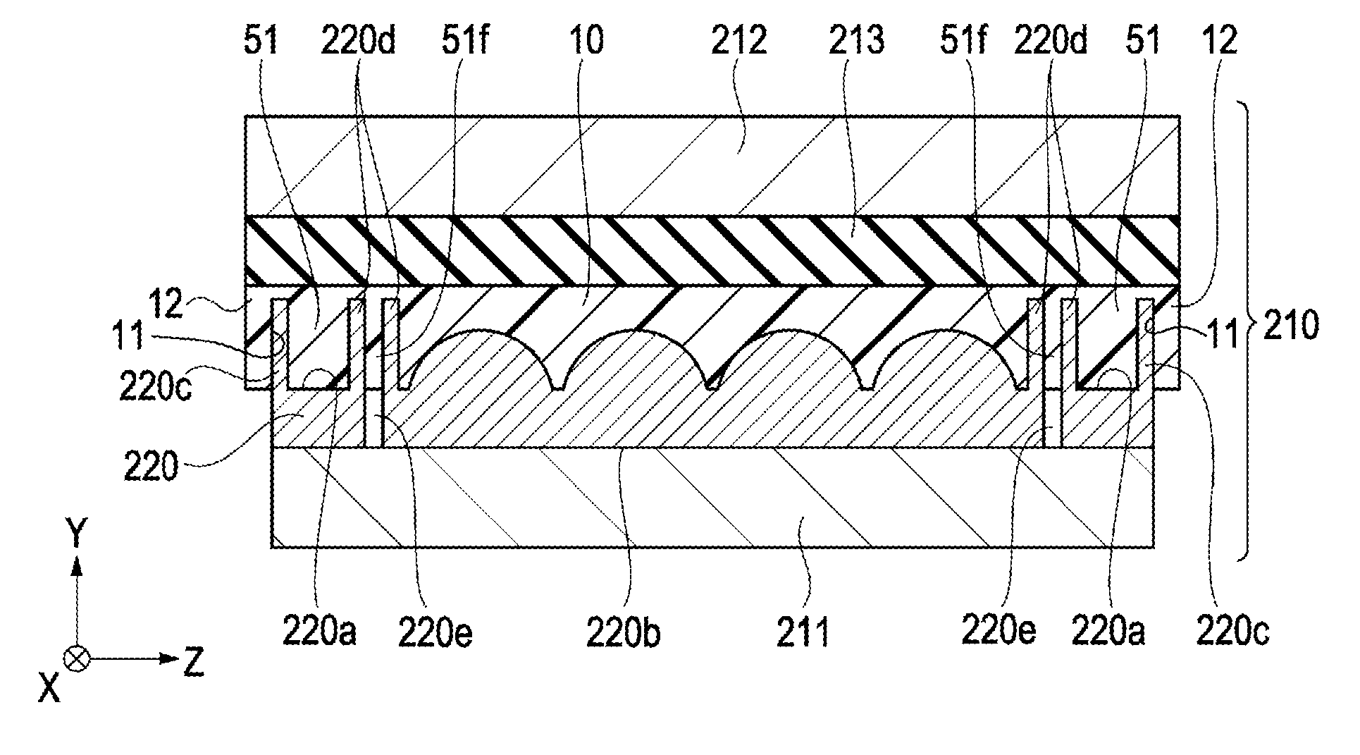
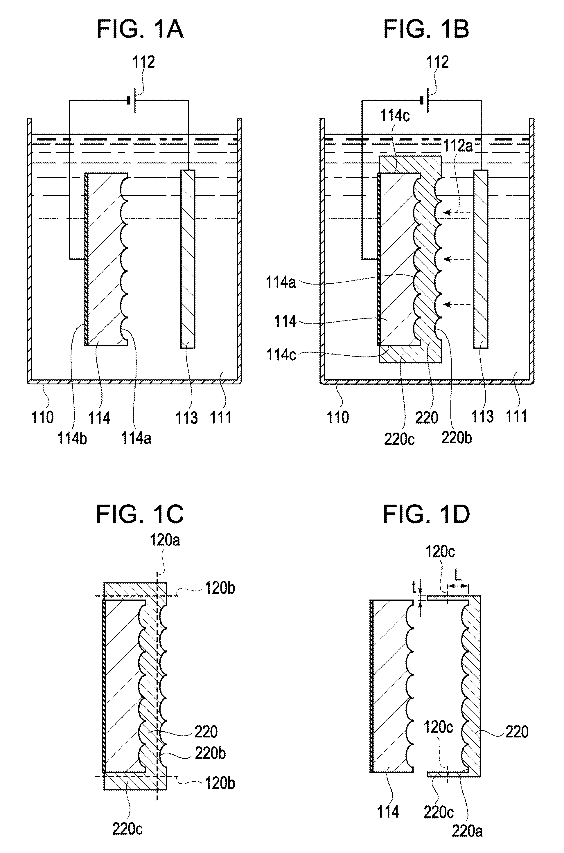
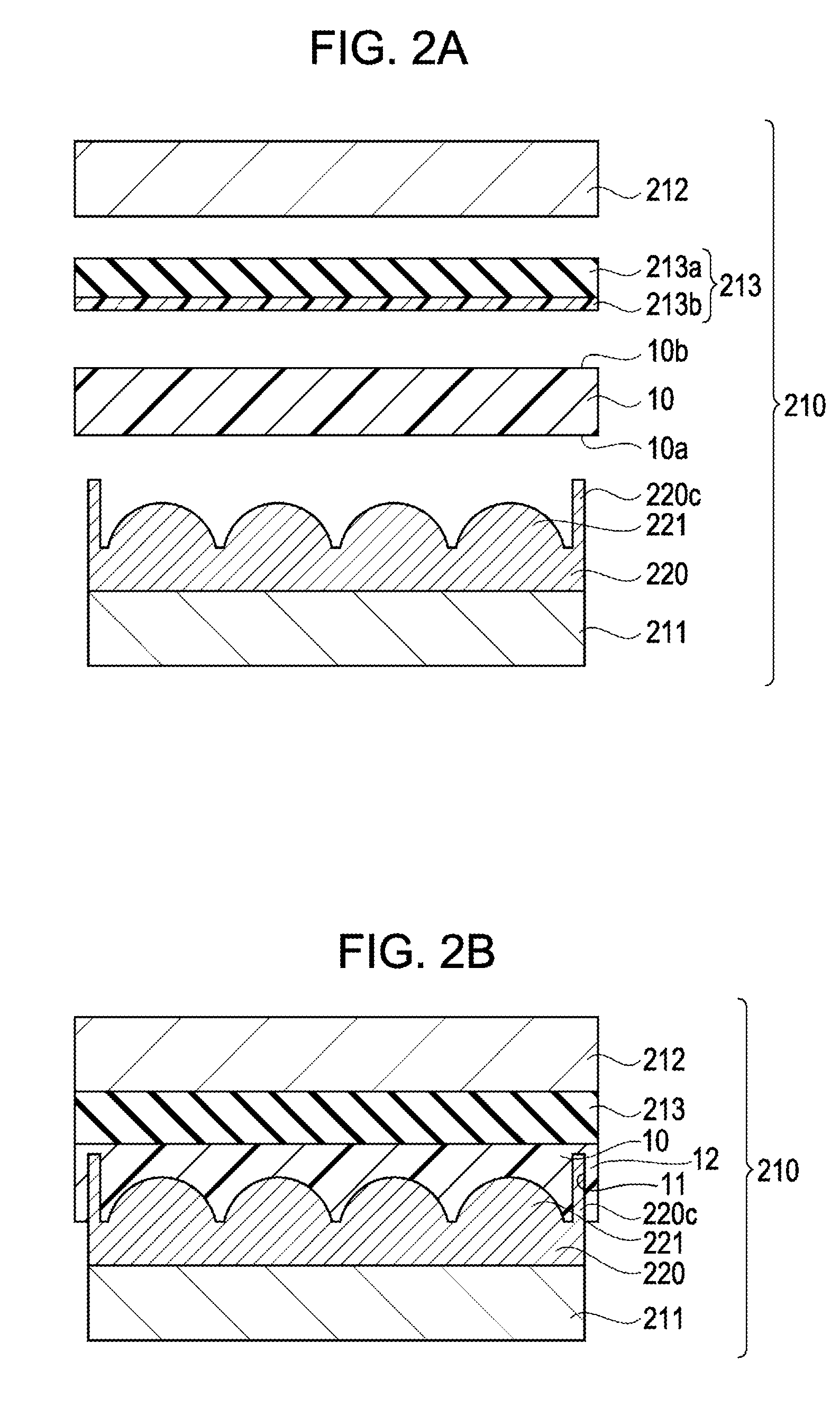
[0027]A method of manufacturing an array substrate 1 according to the embodiment, and the array substrate which is manufactured using the method will be described with reference to FIGS. 1A to 3B. FIGS. 1A to 1D are schematic diagrams which show formation processing of a mold member forming a mold member 220 which deforms a substrate as the array substrate 1. FIGS. 2A and 2B are schematic diagrams which show substrate transfer processing in which the shape of the mold member 220 is transferred to the array substrate. In addition, FIGS. 3A and 3B are schematic diagrams which show the array substrate 1 which is formed using a method of manufacturing an array base material according to the embodiment.

[0028]A method of manufacturing the array substrate 1 in which a concave portion, or a convex portion is formed in an array shape will be described. Mold member formation processing and substrate transfer processing are included in the processing of the method of manufacturing the array su...

second embodiment

[0056]The embodiment is a method of manufacturing a screen including a reflective film which reflects incident light, and which is manufactured using a method of manufacturing the array substrate 1 described in the first embodiment.

[0057]FIG. 4 is a schematic view which shows an installation example of the screen according to the embodiment. FIGS. 5A and 5B are schematic views which show transfer processing of a screen base material which is manufactured using the manufacturing method of the array substrate 1 described in the first embodiment, and the surface of the screen base material. FIG. 6 is a schematic view which shows formation processing of the reflective film of the screen according to the embodiment. In addition, FIGS. 7A and 7B are schematically cross-sectional views which schematically show a part of the screen surface according to the embodiment.

[0058]The method of manufacturing the screen according to the embodiment, and the screen which is manufactured using the meth...

modification example 1

[0076]The array substrate 1 according to the first embodiment is formed with the semicircular convex portion 2c, or the concave portion 1c which is aligned. However, the shape of the array substrate is not limited to this, and may be formed with a polygonal semicircular convex portion 2c, or the concave portion 1c which is aligned.


PUM

PropertyMeasurementUnit
Thicknessaaaaaaaaaa
Thermoplasticityaaaaaaaaaa

Abstract

A plurality of convex portions, or concave portions which is transferred in an array shape, and a groove are transferred with respect to the substrate having thermoplasticity by a mold member having shapes of the convex portion, or the concave portion, and a protruding portion as the groove, and substrate transfer processing is included, in which the convex portion, or concave portion, and a protruding portion which are formed in the mold member are transferred to the substrate by pressing the mold member to the substrate.

Description

BACKGROUND[0001]1. Technical Field[0002]The present invention relates to a method of manufacturing an array substrate, a method of manufacturing an array substrate and a screen, and a screen.[0003]2. Related Art[0004]In the related art, an array substrate in which a plurality of small convex portions, or concave portions is formed to be arrayed has been applied to a screen on which an image is displayed by reflecting projection light which is emitted from a projection-type display device such as a projector. It is known that, in these array substrates, it is possible to use an imprint molding method (hereinafter, referred to as “transfer molding method”) as a method of molding resin as a raw material, and to easily form a screen which causes the projection light to be reflected.[0005]In a method of manufacturing the Fresnel lens using hot press (transfer molding method), regarding a method of forming a molding die, a method is disclosed in JP-A-5-156484, in which a conductive resin ...

Claims


Application Information

Patent Timeline
IPC IPC(8): G03B21/56B05D5/06C25D1/10B29D11/00G02B5/08G03B21/60
CPCB29D11/00298C25D1/10B29C43/021G02B17/002G03B21/602G02B5/0257G02B5/0268G02B5/0284G02B5/0215
Inventor SAITO, ATSUSHI
Owner SEIKO EPSON CORP
Learn More