Sidewall image transfer process employing a cap material layer for a metal nitride layer

a metal nitride layer and image transfer technology, applied in the direction of semiconductor/solid-state device manufacturing, basic electric elements, electric apparatus, etc., can solve the problems of loss or distortion of transfer pattern fidelity, and achieve high-fidelity reproduction

Inactive Publication Date: 2012-11-08
INT BUSINESS MASCH CORP
View PDF7 Cites 174 Cited by
  • Summary
  • Abstract
  • Description
  • Claims
  • Application Information

AI Technical Summary

Benefits of technology

[0003]A cap material layer is deposited on a metal nitride layer. An antireflective coating (ARC) layer, an organic planarizing layer (OPL), and patterned line structures are formed upon the cap material layer. The pattern in the patterned line structures is transferred into the ARC layer and the OPL. Exposed portions of the cap material layer are etched simultaneously with the etch removal of the patterned line structures and the ARC layer. The OPL and the dielectric cap material layer are employed to etch the metal nitride layer. The patterned cap material layer located over the metal nitride layer protects the top surface of the metal nitride layer, and enables high fidelity reproduction of the pattern in the metal nitride layer without pattern distortion. The metal nitride layer is subsequently employed as an etch mask for pattern transfer into an underlying layer.

Problems solved by technology

The OPL tends to be consumed during the pattern transfer into the titanium nitride layer, resulting in distortion or loss of fidelity in the transferred pattern in the titanium nitride layer.

Method used


Image

  • Sidewall image transfer process employing a cap material layer for a metal nitride layer
  • Sidewall image transfer process employing a cap material layer for a metal nitride layer
  • Sidewall image transfer process employing a cap material layer for a metal nitride layer

Examples


first embodiment

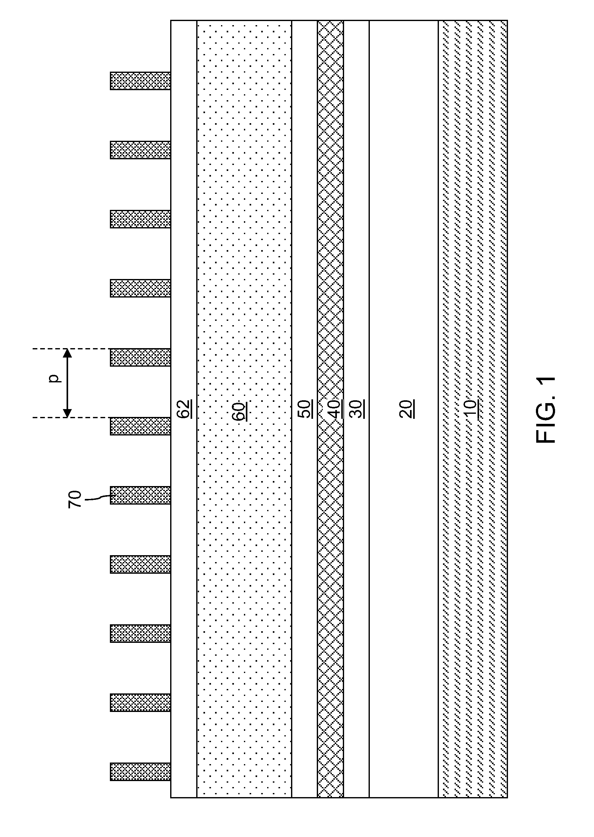
[0023]Referring to FIG. 1, a first exemplary structure according to the present disclosure includes a substrate 10 and a material stack formed thereupon. The substrate 10 can include a semiconductor substrate having semiconductor devices (not shown) therein. The semiconductor devices can include, for example, field effect transistors, junction transistors, diodes, resistors, capacitors, inductors, or any other semiconductor device known in the art. The substrate 10 may, or may not, include contact-level dielectric material layers (not shown) and / or interconnect level dielectric material layers (not shown) as well as embedded contact via structures (not shown) and / or embedded wiring level metal interconnect structures. Alternately, the topmost portion of the substrate 10 can include a semiconductor material such as single crystalline silicon.

[0024]An underlying material layer 20 can be formed on the substrate 10. The underlying material layer 20 can be a single dielectric material la...

second embodiment

[0060]Referring to FIG. 12, a second exemplary structure according to the present disclosure can be derived from the first exemplary structure by extending the duration of the etch and the depth of the trenches 21 at a processing step corresponding to FIG. 10. The trenches 21 are extended to the bottom of the underlying material layer 20 at the end of the etch step.

[0061]Referring to FIG. 13, conductive line structures 22 are formed within the underlying material layer 20 employing the same processing steps as in the first embodiment.

third embodiment

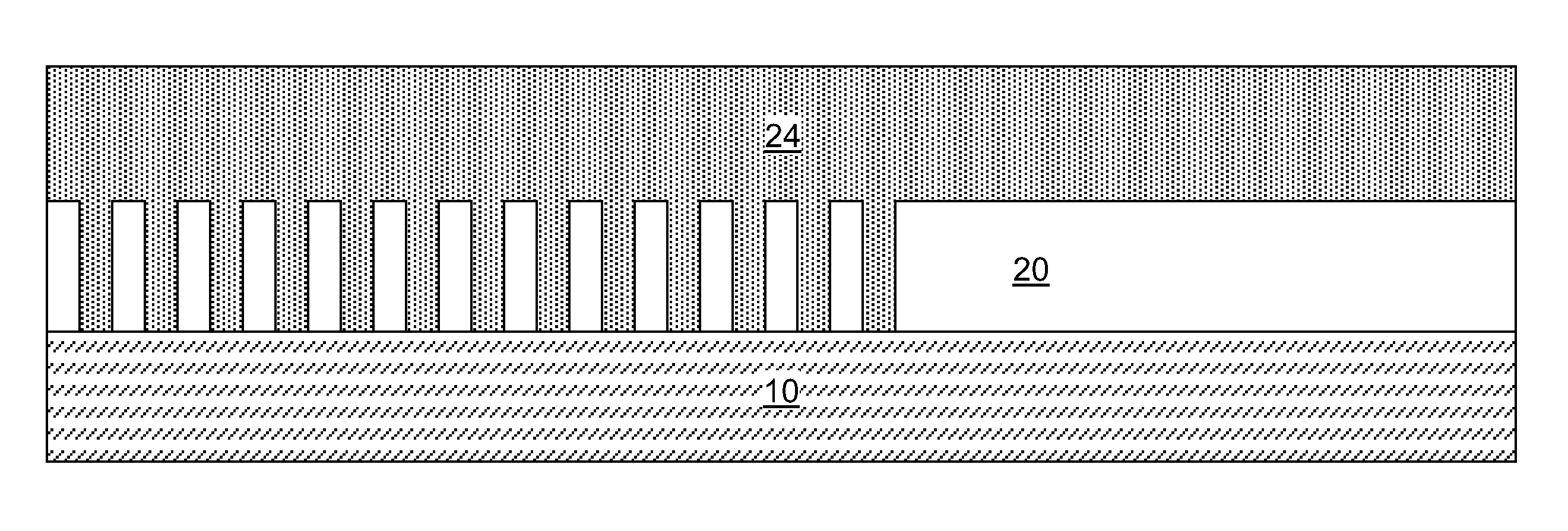
[0062]Referring to FIG. 14, in a third exemplary structure according to the present disclosure, the underlying material layer 20 can include a conductive material. The trenches 21 are formed through the underlying material layer 20 to the top surface of the substrate 10, which may include a dielectric surface. The underlying material layer 20 can be patterned into multiple conductive portions that do not contact one another.

[0063]Referring to FIG. 15, a dielectric material layer 24 can be deposited over the patterned underlying material layer 20 to provide electrical isolation between the various conductive portions of the patterned underlying material layer 20. Optionally, additional conductive structures (not shown) may be formed in an upper portion of the dielectric material layer 24 to provide electrical connections among the various conductive portions of the underlying material layer 20.


PUM

PropertyMeasurementUnit
thicknessesaaaaaaaaaa

Abstract

A cap material layer is deposited on a metal nitride layer. An antireflective coating (ARC) layer, an organic planarizing layer (OPL), and patterned line structures are formed upon the cap material layer. The pattern in the patterned line structures is transferred into the ARC layer and the OPL. Exposed portions of the cap material layer are etched simultaneously with the etch removal of the patterned line structures and the ARC layer. The OPL is employed to etch the metal nitride layer. The patterned cap material layer located over the metal nitride layer protects the top surface of the metal nitride layer, and enables high fidelity reproduction of the pattern in the metal nitride layer without pattern distortion. The metal nitride layer is subsequently employed as an etch mask for pattern transfer into an underlying layer.

Description

BACKGROUND[0001]The present disclosure generally relates to a process for manufacturing semiconductor structures, and particularly to methods for sidewall image transfer employing a dielectric cap material layer on top of a metal nitride layer.[0002]A sidewall image transfer (SIT) process as known in the art employs a titanium nitride layer as an etch mask for transferring a composite image of two independent images. An organic planarizing layer (OPL) is formed directly on the titanium nitride layer, and is consumed during the transfer of the composite pattern into the titanium nitride layer. The OPL tends to be consumed during the pattern transfer into the titanium nitride layer, resulting in distortion or loss of fidelity in the transferred pattern in the titanium nitride layer. A method of enhancing the fidelity of pattern transfer during a SIT process is desired.BRIEF SUMMARY[0003]A cap material layer is deposited on a metal nitride layer. An antireflective coating (ARC) layer, ...

Claims


Application Information

Patent Timeline
Patent Type & Authority Applications(United States)
IPC IPC(8): H01L21/302
CPCH01L21/0337H01L21/31144H01L21/76816H01L21/76885H01L21/32139
Inventor ARNOLD, JOHN C.BURNS, SEAN D.COLBURN, MATTHEW E.HORAK, DAVID V.YIN, YUNPENG
Owner INT BUSINESS MASCH CORP
Why Eureka
Try Eureka