Method for storing wafers

Inactive Publication Date: 2012-11-15
NAN YA TECH
View PDF33 Cites 2 Cited by
  • Summary
  • Abstract
  • Description
  • Claims
  • Application Information

AI Technical Summary

Benefits of technology

[0006]One object of the present invention is to provide a method for storing wafers to prolong Q time.

Problems solved by technology

However, the ultra-pure nitrogen gas is costly.

Method used


Image

  • Method for storing wafers
  • Method for storing wafers
  • Method for storing wafers

Examples


Embodiment Construction

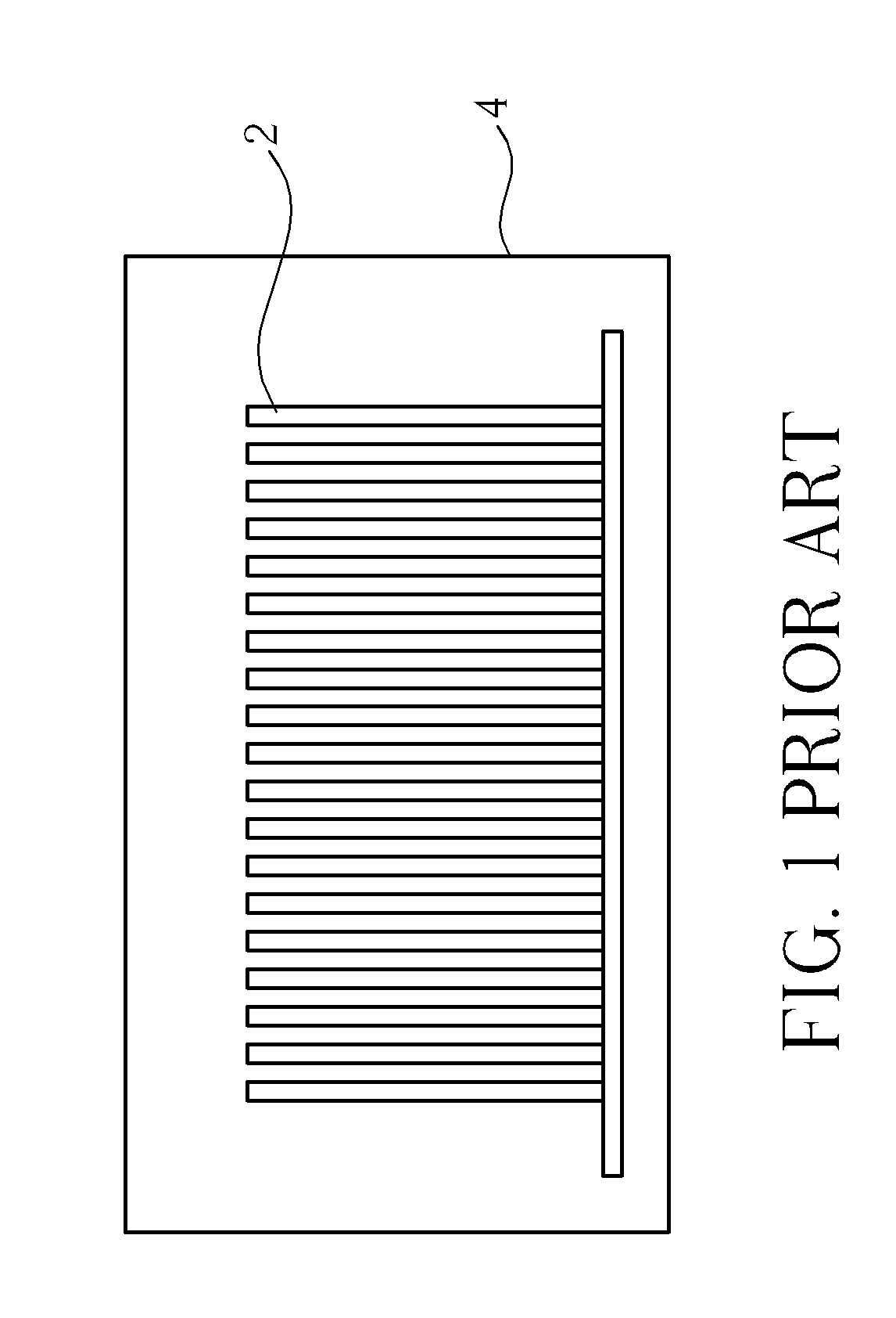
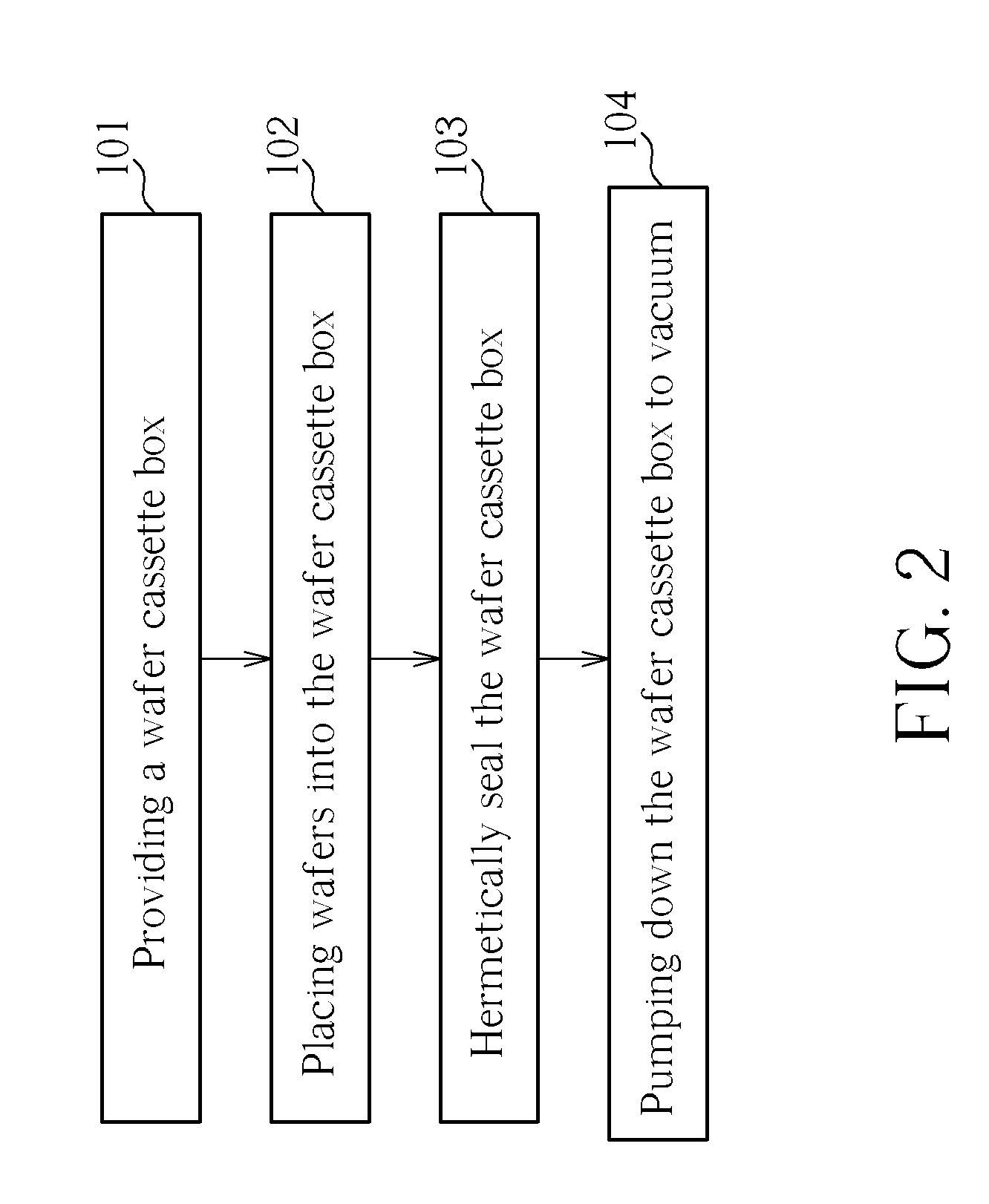
[0016]Referring to FIG. 2 and FIG. 3, a method for storing wafers according to an embodiment includes steps described as follows. First, Step 101 is performed to provide a wafer cassette box. The wafer cassette box 10 may include a box body 12 having an opening and a cover member 14 for closing the opening. The wafer cassette box 10 may be a conventional one. The cover member 14 can be used to hermetically cover the opening to allow the wafer cassette box 10 to be in an airtight status. The wafer cassette box 10 has a valve 18 for pumping. The valve 18 may be disposed on the box body 12 or the cover member 14.

[0017]Next, Step 102 is performed to place wafers 20 into the wafer cassette box 10 through the opening of the wafer cassette box 10. The wafers 20 may be semi-products processed from a semiconductor device manufacturing process and wait for a subsequent process. The wafers 20 may be usually carried by a holder 22. The wafers 20 and the holder 22 may be put together into the wa...


PUM


Abstract

A method for storing wafers is disclosed. A plurality of wafers are placed into the wafer cassette box. The wafer cassette box is hermetically sealed and pumped down to vacuum for the wafer storage. Alternatively, the wafers carried by a holder conveyed on a wafer conveyor are placed into a pump-down chamber enclosing a section of the wafer conveyor. The pump-down chamber is hermetic sealed and pumped down to vacuum for the wafer storage on the wafer conveyor.

Description

BACKGROUND OF THE INVENTION[0001]1. Field of the Invention[0002]The present invention relates to a method of fabricating semiconductor devices, and particularly to a method of storing wafers in the interval of two semiconductor manufacturing processes.[0003]2. Description of the Prior Art[0004]In the semiconductor fabrication technology, extremely high cleanliness environment is demanded for wafer processing. The wafers for processing and loading / unloading to / from a process tool are constantly flushed with ultra-pure nitrogen that contains no oxygen and moisture, in order to eliminate micro-contamination and to reduce native oxide growth on silicon surfaces. During a Q-time between two fabricating processes, as shown in FIG. 1, wafers 2 are usually stored in a wafer storage container 4 without the particle contamination, moisture absorption and oxidation problems by maintaining a positive pressure of an inert gas (such as nitrogen gas) inside the container higher than the surroundin...

Claims


Application Information

Patent Timeline
IPC IPC(8): H01L21/677B65B31/00
CPCH01L21/67393
Inventor HSIEH, MING-TENGCHEN, YI-NANLIU, HSIEN-WEN
Owner NAN YA TECH
Why Eureka
Try Eureka