Method for manufacturing solid-state image pickup device
a solid-state image and pickup device technology, applied in semiconductor/solid-state device manufacturing, semiconductor devices, electrical equipment, etc., can solve the problems of polysilicon film undetected in narrow spaces, degradation of image quality, charge leakage, etc., and achieve the effect of improving yield
- Summary
- Abstract
- Description
- Claims
- Application Information
AI Technical Summary
Benefits of technology
Problems solved by technology
Method used
Image
Examples
first embodiment
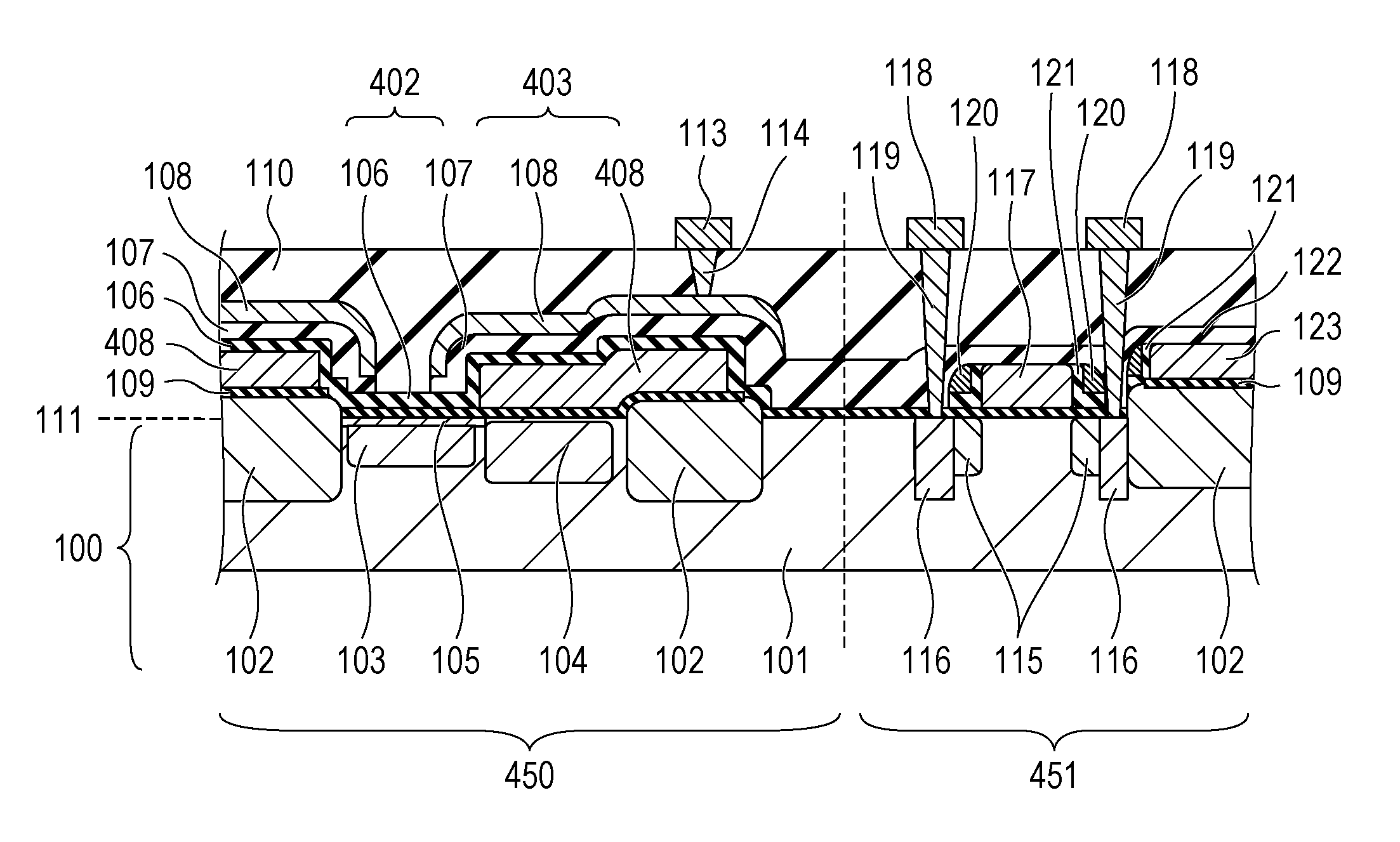
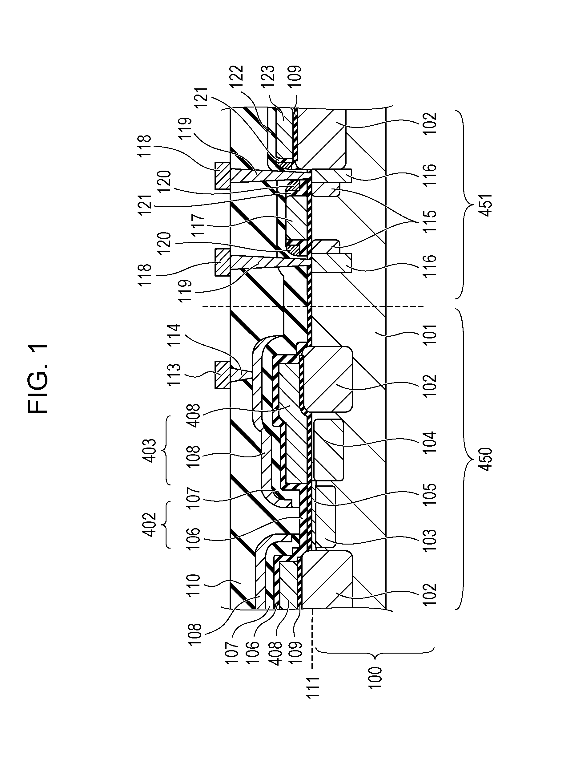
[0020]A solid-state image pickup device according to a first embodiment will be described using FIGS. 1, 4, and 5.
[0021]FIG. 1 is a schematic sectional view of the solid-state image pickup device according to this embodiment. FIG. 4 illustrates a circuit diagram of four pixels included in the solid-state image pickup device according to this embodiment. FIG. 5 is a schematic plan view corresponding to FIG. 4.
[0022]First, the description will be given of FIG. 4 illustrating a circuit diagram of four pixels of the solid-state image pickup device according to this embodiment and FIG. 5 illustrating a schematic plan view that corresponds to FIG. 4. FIG. 4 illustrates a configuration in which pixels 413 each having a charge holding part are arranged in a 2×2 matrix form. In this embodiment, each pixel 413 includes a photoelectric conversion element 402, a charge holding part 403, a floating diffusion part 404, a power supply part 405, a pixel output part 407, a first gate electrode 408 o...
second embodiment
[0038]As in the first embodiment, a solid-state image pickup device according to a second embodiment relates a solid-state image pickup device having light-shielding films. Unlike the first embodiment, the solid-state image pickup device according to this embodiment relates to a solid-state image pickup device having pixels for acquiring image signals and pixels for acquiring focus detection signals in the pixel portion 450. The solid-state image pickup device according to this embodiment will be described using FIGS. 6A to 7.
[0039]FIG. 6A illustrates a circuit diagram of a pixel 713 of the solid-state image pickup device according to this embodiment. In this embodiment, the pixel 413 of the solid-state image pickup device according to the first embodiment illustrated in FIG. 4 is replaced with the pixel 713 illustrated in FIG. 6A. The pixel 713 illustrated in FIG. 6A has a circuitry of a general CMOS solid-state image pickup device. Specifically, the pixel 713 includes a photoelect...
PUM
| Property | Measurement | Unit |
|---|---|---|
| thickness | aaaaa | aaaaa |
| thickness | aaaaa | aaaaa |
| insulating | aaaaa | aaaaa |
Abstract
Description
Claims
Application Information


