Light-emitting diode with strain-relaxed layer

a light-emitting diode and strain-relaxed technology, which is applied in the manufacture of semiconductor/solid-state devices, semiconductor devices, electrical apparatus, etc., can solve the problems of reducing the iqe, drooping effect, and undesirable built-in electric field of led which employs nitride films along the polar c-direction of a sapphire substra

Active Publication Date: 2012-12-06
EPISTAR CORP
View PDF1 Cites 4 Cited by
  • Summary
  • Abstract
  • Description
  • Claims
  • Application Information

AI Technical Summary

Problems solved by technology

For example, an LED which employs nitride films grown along the polar c-direction of a sapphire substrate suffers from the undesirable built-in electric field.
The built-in electric field not only reduces the IQE, but also results in the droop effect.

Method used


Image

  • Light-emitting diode with strain-relaxed layer
  • Light-emitting diode with strain-relaxed layer
  • Light-emitting diode with strain-relaxed layer

Examples


Embodiment Construction

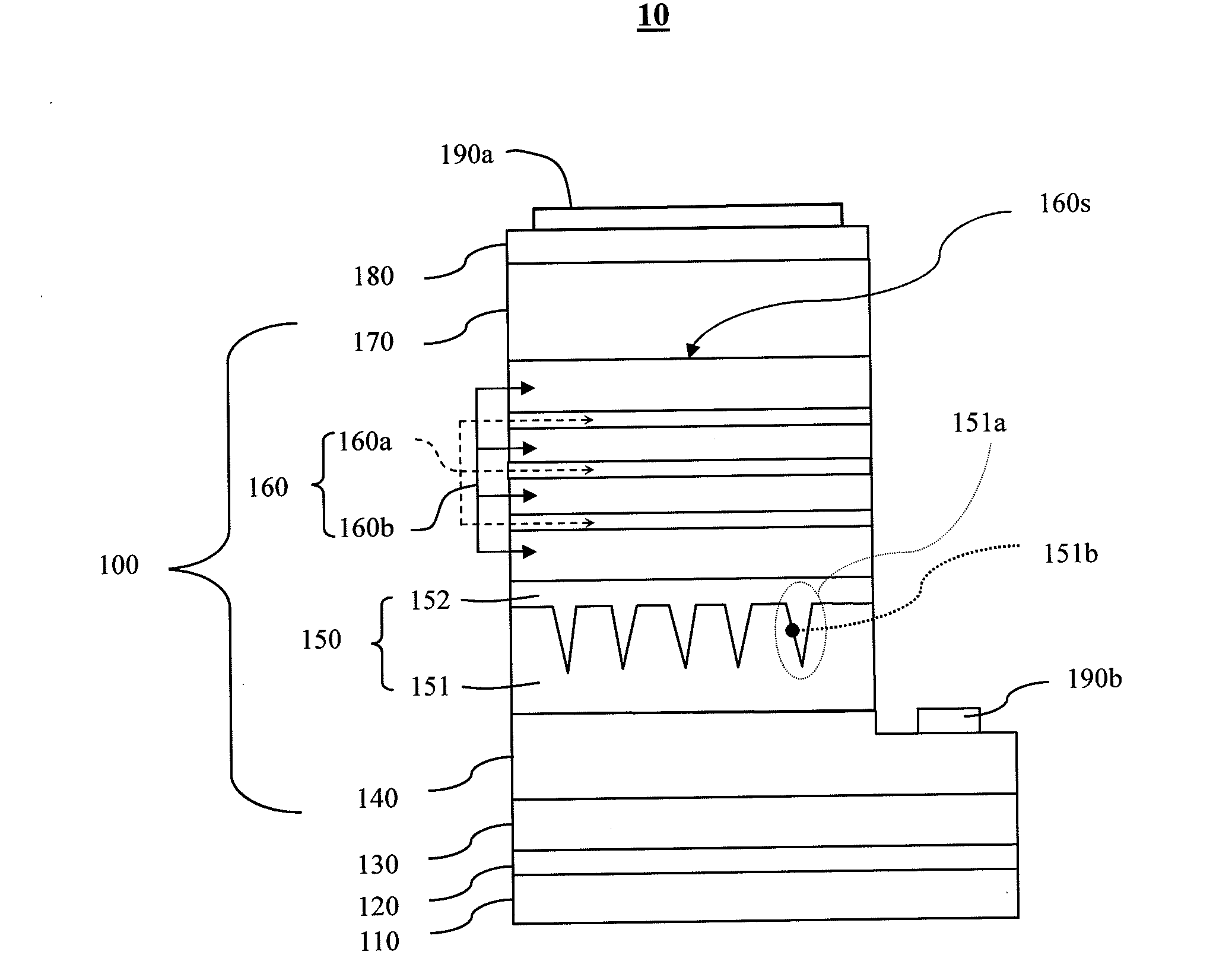
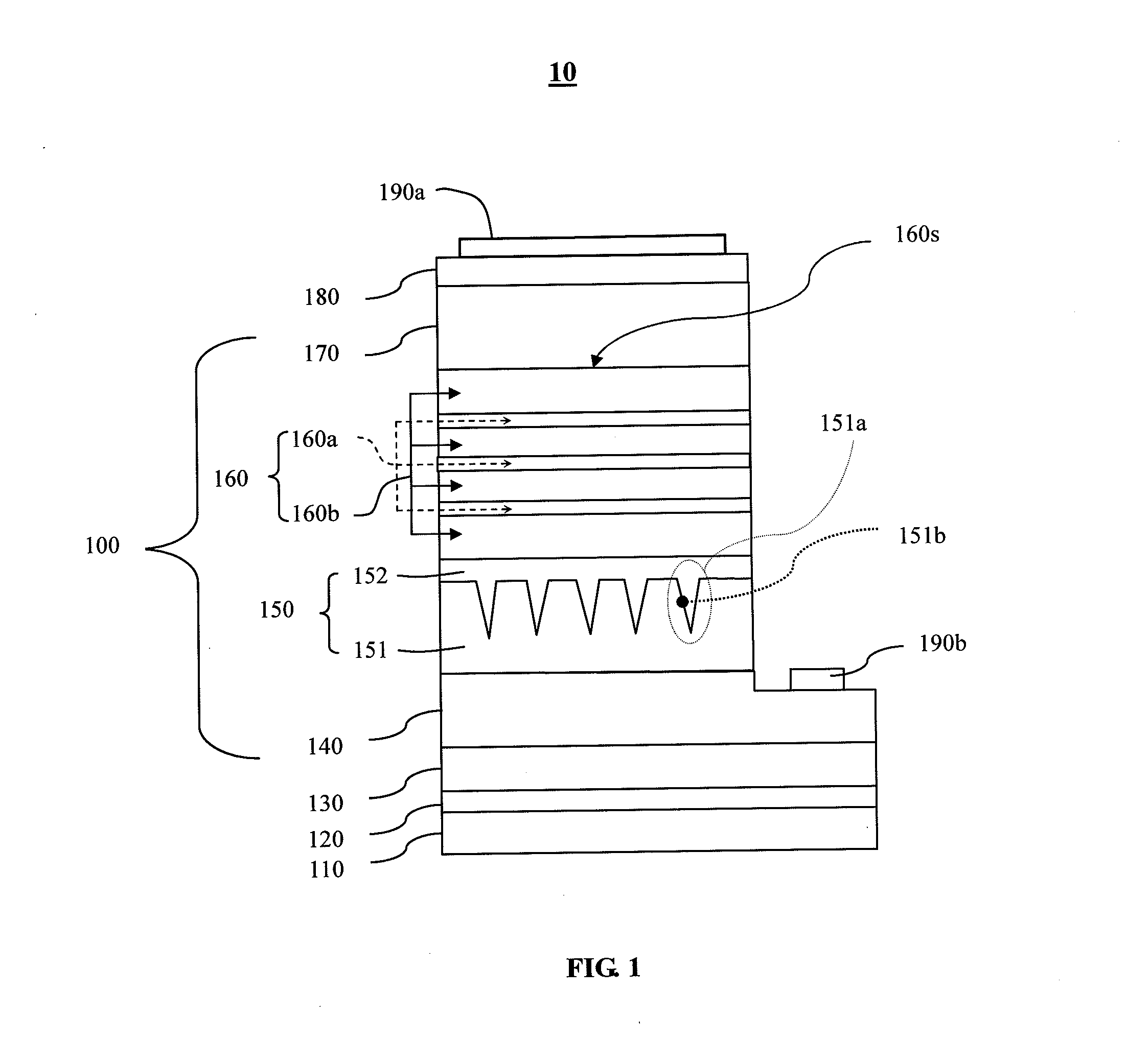
[0009]FIG. 1 illustrates an embodiment of present application. The light-emitting diode 10 is formed on a substrate 110, for example, a sapphire substrate. On the substrate 110, a buffer layer 120 is formed. The buffer layer 120 is a layer of GaN or AlN grown at a temperature, for example, 500° C.˜650° C. On the buffer layer 120, an un-doped GaN layer 130 is formed. On the un-doped GaN layer 130, a main structure 100 is formed.

[0010]The main structure 100 in this embodiment includes a first conductivity type semiconductor layer 140, a second conductivity type semiconductor layer 170. For example, the first conductivity type semiconductor layer 140 is n-type, and the second conductivity type semiconductor layer 170 is p-type. And between the first conductivity type semiconductor layer 140 and the second conductivity type semiconductor layer 170, an active layer 160 is disposed. An example for the active layer 160 is a multi-quantum well structure comprising a plurality of quantum wel...


PUM


Abstract

Disclosed is a light-emitting diode (LED) and the method to form the LED. The LED comprises: a first conductivity type semiconductor layer; a strain-relaxed layer over the first conductivity type semiconductor layer, the strain-relaxed layer comprising: a strain-absorbed layer over the first conductivity type semiconductor layer, the strain-absorbed layer containing a plurality of cavities in a substantial hexagonal-pyramid form; and a surface-smoothing layer on the strain-absorbed layer filling the cavities; an active layer over the strain-relaxed layer; and a second conductivity type semiconductor layer over the active layer.

Description

TECHNICAL FIELD[0001]The application relates to a light-emitting device, in particular to a light-emitting diode with strain-relaxed layer.DESCRIPTION OF BACKGROUND ART[0002]The theory for a light-emitting diode (LED) to emit light is that when a forward voltage power is applied to a p-n junction, the electrons are driven from the n-type semiconductor and the holes are driven from the p-type semiconductor, and these carriers are combined in the active layer to emit light. The efficiency of an LED depends on the Internal Quantum Efficiency (IQE), which depends on the combination rate of the electrons from the n-type semiconductor and the holes from the p-type semiconductor. However, the IQE is reduced by the built-in electric field. The built-in electric field is an effect due to the piezoelectric polarizations as a result of the characteristics of the materials used for LED. For example, an LED which employs nitride films grown along the polar c-direction of a sapphire substrate suf...

Claims


Application Information

Patent Timeline
Patent Type & Authority Applications(United States)
IPC IPC(8): H01L33/06H01L33/12
CPCH01L21/02458H01L21/02505H01L21/02513H01L21/0254H01L33/32H01L33/08H01L33/12H01L33/22H01L33/007
Inventor LEE, SHIH-CHANG
Owner EPISTAR CORP
Why Eureka
Try Eureka